Method for lithograghic patterning of sensitive materials

a sensitive material and lithography technology, applied in the field of submicron patterning of organic materials, can solve the problems of difficult photolithographic patterning, difficult stamp-based lithography and active approaches, and unreliable reliability, and achieve the effect of avoiding exposure of sensitive materials

a sensitive material and lithography technology, applied in the field of submicron patterning of organic materials, can solve the problems of difficult photolithographic patterning, difficult stamp-based lithography and active approaches, and unreliable reliability, and achieve the effect of avoiding exposure of sensitive materials

US10581003B2Active Publication Date: 2020-03-03THE BOARD OF TRUSTEES OF THE LELAND STANFORD JUNIOR UNIV

Image

  • Method for lithograghic patterning of sensitive materials
  • Method for lithograghic patterning of sensitive materials
  • Method for lithograghic patterning of sensitive materials

Examples


Embodiment Construction

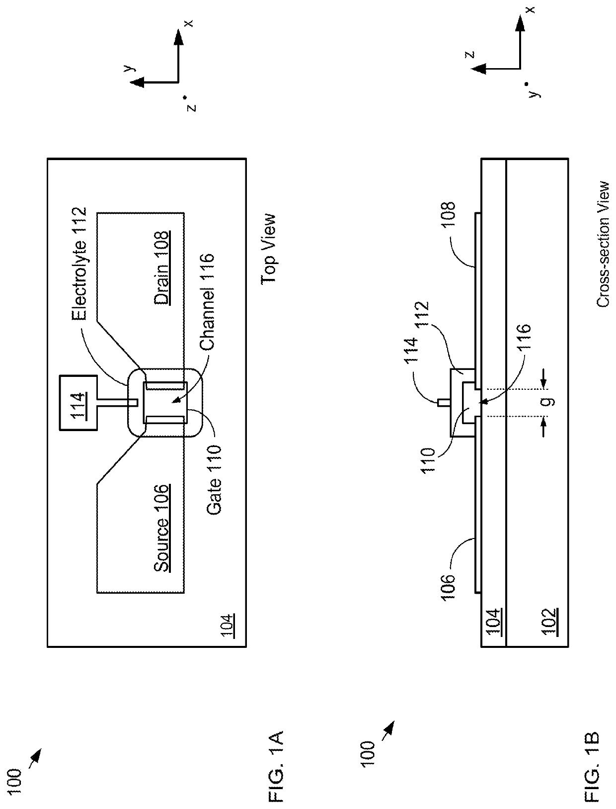
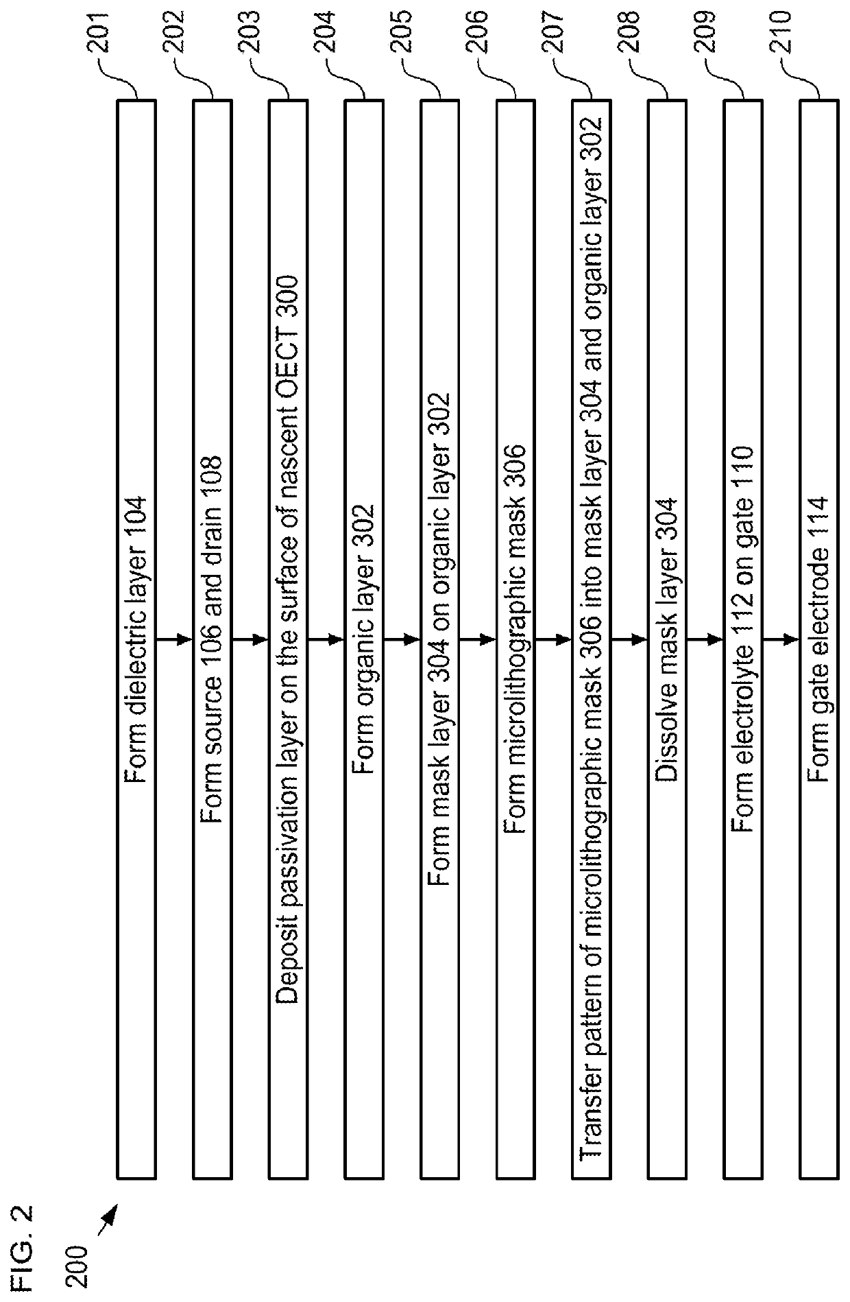
[0026]FIGS. 1A and 1B depict schematic drawings of top and cross-sectional views, respectively, of an organic-semiconductor device formed via a fabrication process in accordance with the present invention. Device 100 is an organic electrochemical transistor that includes substrate 102, dielectric layer 104, source 106, drain 108, gate 110, electrolyte 112, and gate electrode 114.

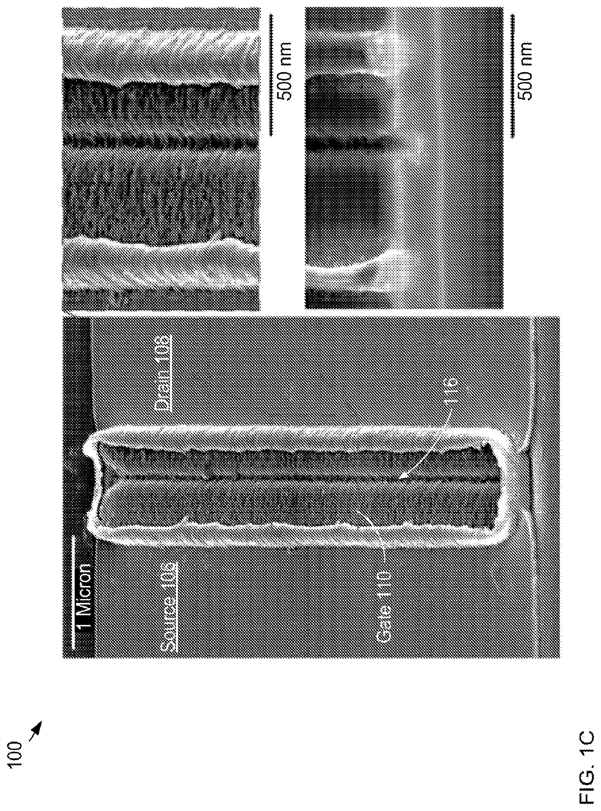
[0027]FIG. 1C depicts photographs of a portion of device 100 at different magnification scales.

[0028]An organic electrochemical transistor, such as device 100, is a special type of electrolyte-gated transistor (EGT). EGTs are attractive for use in sensing applications not only due to their low turn-on voltage and relatively high transconductance, but also because they can be miniaturized using substantially standard fabrication processes. The device structure of an EGT is analogous to that of a regular field effect transistor (FET); however, in an EGT, the solid insulating layer of the conventional FET is re...


PUM

PropertyMeasurementUnit
thicknessaaaaaaaaaa
thicknessesaaaaaaaaaa

Abstract

Methods for patterning highly sensitive materials, such as organic materials, organic semiconductors, biomolecular materials, and the like, with photolithographic resolution are disclosed. In some embodiments, a germanium mask (304) is formed on the surface of the sensitive material (302), thereby protecting it from subsequent processes that employ harsh chemicals that would otherwise destroy the sensitive material (302). A microlithography mask (306) is patterned on the germanium mask layer (304), after which the germanium exposed by the microlithography mask (306) is removed by dissolving it in water. After transferring the pattern of the germanium mask (304) into the sensitive material (302), the germanium and microlithography masks (304, 306) are completely removed by immersing the substrate in water, which dissolves the remaining germanium and lifts off the microlithography mask material. As a result, the only chemical to which the sensitive material (302) is exposed during the patterning process is water, thereby mitigating or avoiding damage to the material (302).

Description

STATEMENT OF RELATED CASES[0001]This case claims priority to U.S. Provisional Patent Application Ser. No. 62 / 383,096, filed Sep. 2, 2016, which is incorporated herein by reference.STATEMENT REGARDING FEDERALLY SPONSORED RESEARCH[0002]This invention was made with Government support under contract DE-AC02-76SF00515 awarded by the Department of Energy. The Government has certain rights in the invention.FIELD OF THE INVENTION[0003]The present invention relates to the patterning of organic materials in general, and, more particularly, to sub-micron patterning of organic materials.BACKGROUND OF THE INVENTION[0004]Organic materials, such as organic semiconductors, have become important materials in many microelectronic applications—from high-performance electronics systems to flat-panel displays based on organic-light-emitting-diodes (OLEDs).[0005]Unfortunately, organic materials are exemplary of a class of sensitive materials that are difficult to pattern photolithographically due to the ...

Claims


Application Information

Patent Timeline
03 Mar 2020
Publication
US10581003B2
IPC
H01L51/05; H01L51/00; G03F7/40; G03F7/42; H01L51/10; H10K99/00
CPC
H01L51/0016; H01L51/102; H01L51/0018; H01L51/0541; G03F7/40; H01L51/0037; G03F7/422; H01L51/0043
Inventors
MELOSH, NICHOLAS ALEXANDER; ANGLE, MATT R.