Power semiconductor device with built-in resistor between control electrode and control terminal, and power semiconductor drive system

a technology of semiconductor devices and drives, applied in power conversion systems, climate sustainability, pulse techniques, etc., can solve problems such as non-uniform current flowing through each semiconductor element, and achieve the effect of suppressing gate resistance and suppressing switching loss

Active Publication Date: 2020-03-10
MITSUBISHI ELECTRIC CORP
View PDF11 Cites 0 Cited by
  • Summary
  • Abstract
  • Description
  • Claims
  • Application Information

AI Technical Summary

Benefits of technology

[0009]According to the power semiconductor device, in the first and second semiconductor elements in each of the first phase circuits, with arrangement of a resistor built-in in a gate, an electrical resistance value between the first control terminal and the control electrode can be higher than an electrical resistance value between the second control terminal and the control electrode. Therefore, when the first and second semiconductor elements are connected in parallel and controlled in common among the plurality of first phase circuits, an electrical signal for turning on and off the first or second semiconductor element is input to the first control terminal so that a phenomenon of resonance of a gate voltage can be suppressed without connecting a resistive element with an external line, and hence a difference in current caused between the plurality of first or second semiconductor elements connected in parallel due to a difference in gate voltage can be suppressed. When the first and second semiconductor elements are individually controlled among the plurality of phase circuits, an electrical signal for turning on and off the first and second semiconductor elements is input to the second control terminal so that a gate resistance can be suppressed and switching loss can be suppressed.

Problems solved by technology

Furthermore, due to a difference in length of a line attributed to variation in manufacturing or a layout, such a configuration of the LC resonance circuit that imbalanced LC components are connected in parallel is concerned.
When it becomes difficult to control in unison, voltages at control electrodes (gates) of a plurality of semiconductor elements connected in parallel due to a resonance phenomenon in the LC resonance circuit, a current which flows through each semiconductor element becomes non-uniform and disadvantageous occurrence of concentration of heat generation in a specific semiconductor element is concerned.

Method used


Image

  • Power semiconductor device with built-in resistor between control electrode and control terminal, and power semiconductor drive system
  • Power semiconductor device with built-in resistor between control electrode and control terminal, and power semiconductor drive system
  • Power semiconductor device with built-in resistor between control electrode and control terminal, and power semiconductor drive system

Examples


first embodiment

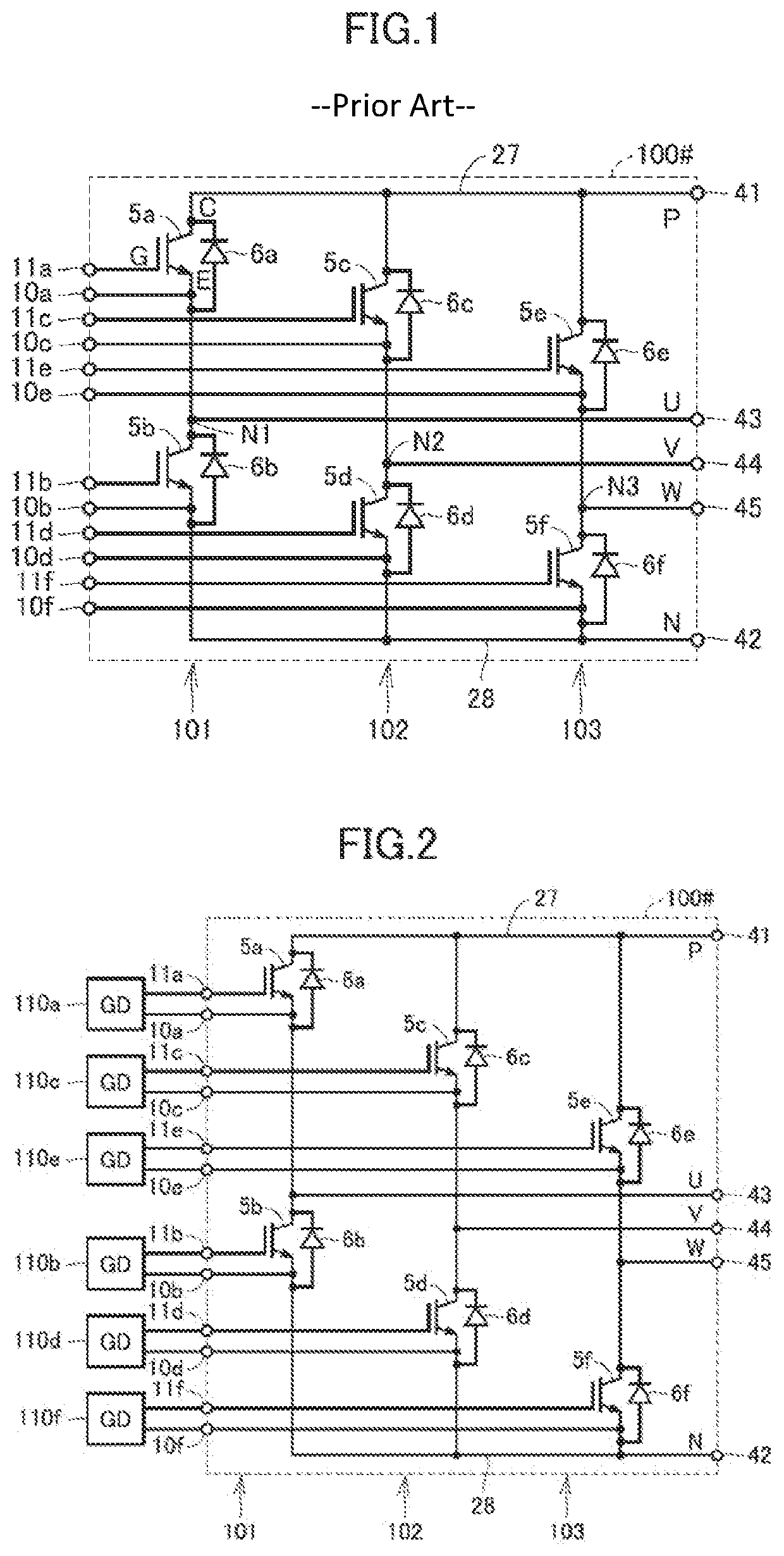
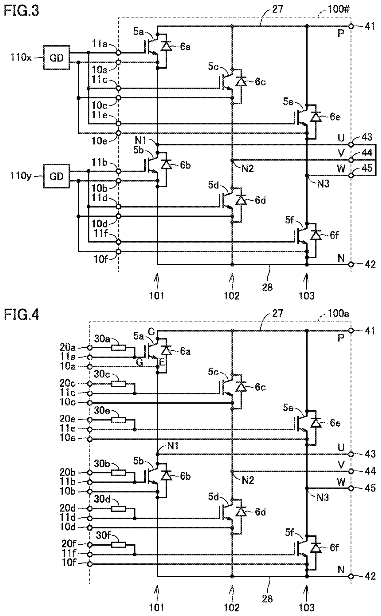
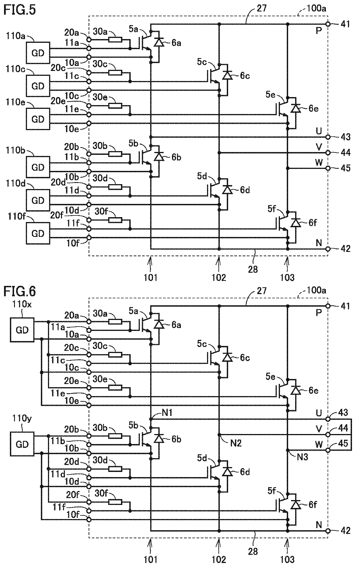
[0035]In the present embodiment, a power semiconductor device mainly for an application as a power conversion device in which a plurality of circuits each corresponding to one phase and constituted of an upper arm and a lower arm connected in series are provided will be described. In particular, a configuration of the power semiconductor device suitable for selective use in a manner that each phase circuit is individually operated and a manner that the upper arm and the lower arm are each operated in common with circuits in a plurality of phases being connected in parallel will be described in detail.

[0036]Though a plurality of semiconductor elements contained in a power semiconductor device will be described in the present embodiment assuming that one semiconductor element is arranged for each arm, each semiconductor element can also actually be configured by connecting a plurality of semiconductor elements in parallel.

first modification

of First Embodiment

[0076]Another example of use in parallel connection of power semiconductor device 100a according to the first embodiment will be described in a first modification of the first embodiment.

[0077]FIG. 7 is a circuit diagram illustrating a manner of use of power semiconductor device 100a shown in FIG. 4, which is different from the first embodiment.

[0078]Referring to FIG. 7, though the configuration of power semiconductor device 100a is the same as in the first embodiment, a manner of connection of control terminals 11a to 11f and 20a to 20f and output terminals 43 to 45 is different from that in the first embodiment. In the first modification of the first embodiment, a boost chopper and a half bridge inverter can be implemented by use in parallel connection of some of semiconductor elements 5a to 5f of power semiconductor device 100a.

[0079]In FIG. 7, output terminals 43 and 44 are short-circuited and connected to a load 115. Thus, in the upper arm, semiconductor ele...

second modification

of First Embodiment

[0086]FIG. 8 is a circuit diagram illustrating a configuration of a power semiconductor device according to a second modification of the first embodiment.

[0087]Referring to FIG. 8, a power semiconductor device 100b according to the second modification of the first embodiment is different from power semiconductor device 100a according to the first embodiment in further including a B-phase circuit 104 and an output terminal 46. Since power semiconductor device 100b is otherwise the same in configuration as power semiconductor device 100a, detailed description will not be repeated.

[0088]B-phase circuit 104 has a semiconductor element 5h and a rectifying element 6g connected in series with an output node N4 being interposed, between power supply lines 27 and 28. In semiconductor element 5h, a terminal 10h and control terminals 11h and 20h as well as a built-in gate resistor 30h are arranged similarly to terminals 10a to 10f and control terminals 11a to 11f and 20a to ...


PUM

PropertyMeasurementUnit
voltageaaaaaaaaaa
electrical resistanceaaaaaaaaaa
electricalaaaaaaaaaa

Abstract

Each of a plurality of semiconductor elements is provided with a first control terminal and a second control terminal. A built-in gate resistor is connected between the semiconductor element and the first control terminal. Individual voltage pulse signals are input to the second control terminals when the plurality of semiconductor elements are individually turned on and off. A common voltage pulse signal is input to some of the first control terminals when a first group of semiconductor elements is turned on and off in common. A common voltage pulse signal is input to others of the first control terminals when a second group of semiconductor elements is turned on and off in common.

Description

BACKGROUND OF THE INVENTIONField of the Invention[0001]This invention relates to a power semiconductor device and a power semiconductor drive system and more particularly to a semiconductor device containing a plurality of semiconductor elements and a system for driving the same.Description of the Background Art[0002]Japanese Patent Laying-Open No. 2012-120304 describes an inverter module containing six power transistors as a semiconductor device containing a plurality of semiconductor elements.SUMMARY OF THE INVENTION[0003]A three-phase inverter is configured such that a semiconductor element defined as an upper arm and a semiconductor element defined as a lower arm in each of a U phase, a V phase, and a W phase are connected in series between power supply lines with an output terminal in each phase being interposed.[0004]Therefore, when output terminals are connected to one another among the plurality of phases, the elements in the upper arm and the elements in the lower arm in th...

Claims


Application Information

Patent Timeline
Patent Type & Authority Patents(United States)
IPC IPC(8): H02M1/084
CPCH02M1/084H03K2217/0009H02M1/32H02M7/5387H02M1/0038H02M1/0054H02M7/53875Y02B70/10
Inventor ISHII, KAZUFUMI
Owner MITSUBISHI ELECTRIC CORP
Why Eureka
Try Eureka