Display substrate, display panel and display device

a display substrate and substrate technology, applied in static indicating devices, instruments, optics, etc., can solve the problems of reducing the production efficiency of the display substrate and the display substrate, reducing the productivity, and damage to the tested display panel, so as to reduce the thickness of the display substrate, reduce the process flow, and improve production efficiency and productivity

Active Publication Date: 2020-03-17
BOE TECH GRP CO LTD +1
View PDF19 Cites 0 Cited by
  • Summary
  • Abstract
  • Description
  • Claims
  • Application Information

AI Technical Summary

Benefits of technology

[0005]In view of the technical problems in the prior art, an object of the present invention is to provide a display substrate, a display panel including the display substrate and a display device including the display panel, wherein a process of coating test pads of the display substrate with UV adhesive can be omitted, so that the production efficiency and the productivity can be improved and the thicknesses of the display substrate, the display panel including the display substrate and the display device including the display panel can be reduced.
[0015]In the display substrate provided by the present invention, the flexible circuit board covers the area of the test pads, so that test points on the test pads can be prevented from contacting the outside, and corrosion of the test points and signal abnormity in signal lines resulting therefrom during testing are prevented; compared with the prior art, the process of coating the test pads with UV adhesive is omitted, thus the process flow is reduced, and the production efficiency and the productivity are improved; moreover, the thickness of the display substrate can be reduced, which is conducive to implementing a lighter and thinner display panel.
[0016]The display panel provided by be present invention adopts the above display substrate provided by the present invention, so that the process of coating the test pads with UV adhesive can be omitted, the process flow is reduced, the production efficiency and the productivity are improved, moreover, the thickness of the display panel can be reduced, which is conducive for the display panel to be lighter and thinner.
[0017]The above display panel provided by the present invention is adopted in the display device provided by the present invention, so that the process of coating the test pads with UV adhesive can be omitted, the process flow is reduced, the production efficiency and the productivity are improved, moreover, the thickness of the display device can be reduced, which is conducive for the display device to be lighter and thinner.

Problems solved by technology

In the above display substrate 1, an exposed conductive metal area on each test pad 2 is generally used as a test point, which is easily corroded in the atmospheric environment, and corrosion of the test point can cause signal abnormity in the signal lines and thus can cause damage to the tested display panel.
Obviously, coating the test pads 2 with the UV adhesive can reduce the production efficiency of the display substrate and the display panel including the display substrate, and reduce the productivity, and also, can result in increased thicknesses of the display substrate and the display panel including the display substrate.

Method used


Image

  • Display substrate, display panel and display device
  • Display substrate, display panel and display device
  • Display substrate, display panel and display device

Examples


Embodiment Construction

[0025]The specific embodiments of the present invention will be described in detail below in conjunction with the accompanying drawings. It should be understood that the specific embodiments described herein are merely used for describing and interpreting the present invention, rather than limiting the present invention.

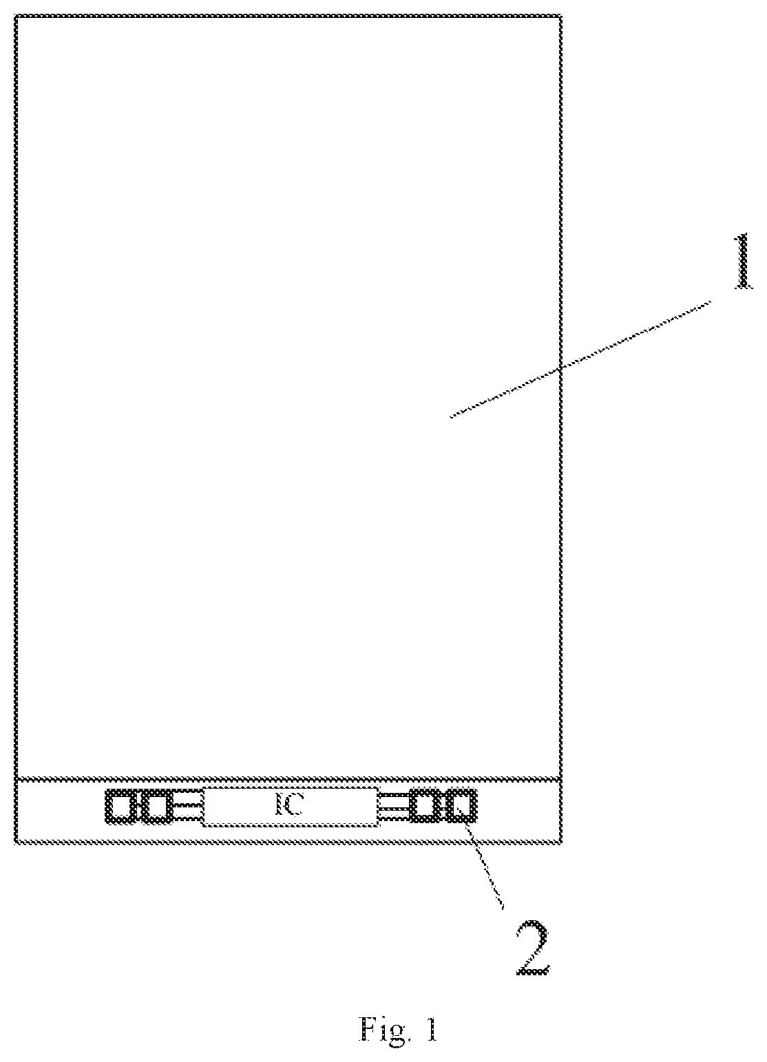
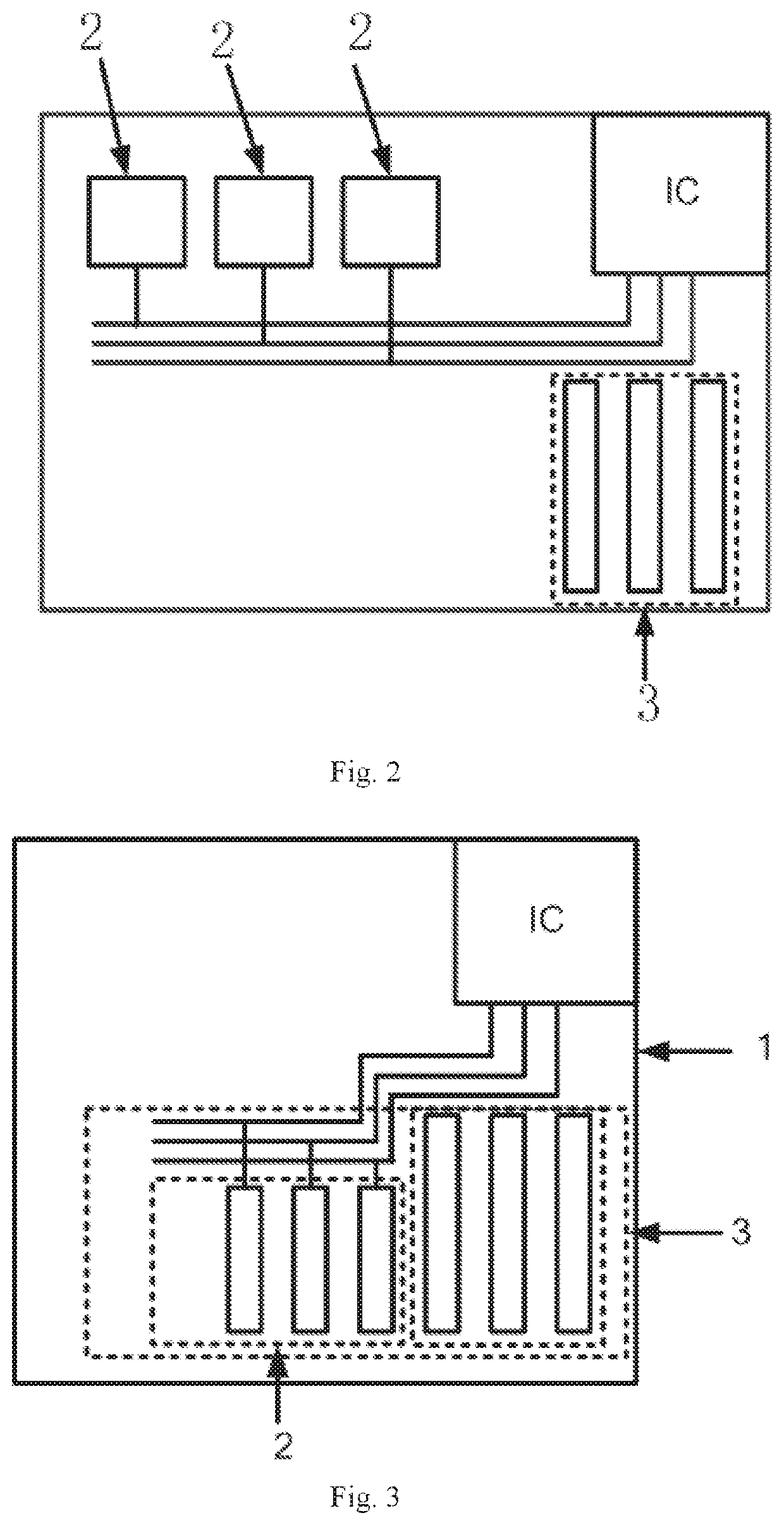
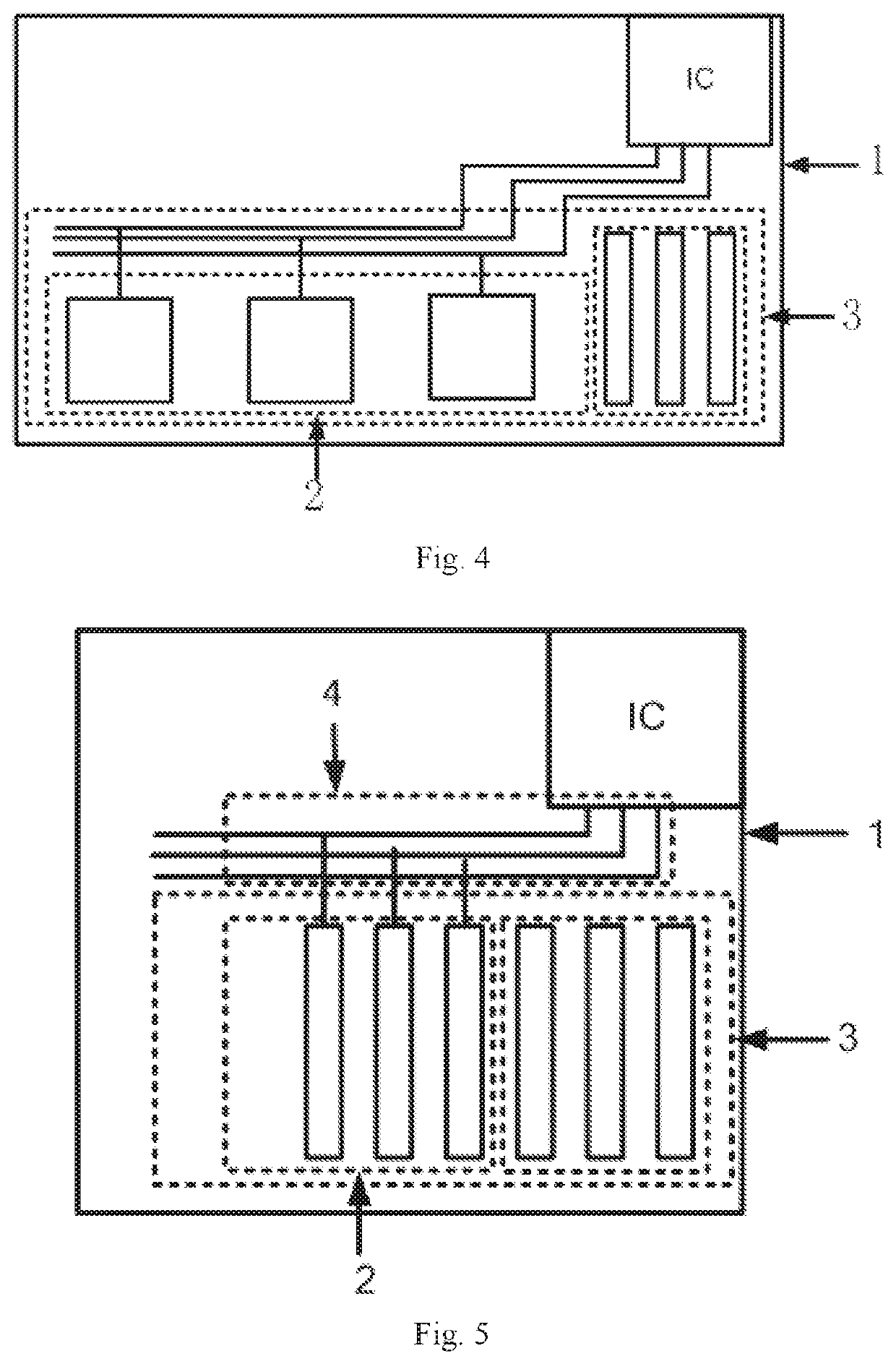
[0026]The present invention provides an embodiment of a display substrate. FIG. 3 is a schematic diagram of a display substrate provided by an embodiment of the present invention. As shown in FIG. 3, the display substrate 1 includes a flexible circuit hoard 3 and test pads 2 in this embodiment, wherein the flexible circuit board 3 covers the area of the test pads 2. Specifically, the display substrate 1 is generally an array substrate.

[0027]In manufacture of the display substrate, after thin film transistors, pixel electrodes and signal lines such as gate lines, data lines and the like are manufactured, test probes are brought into contact with test points on the tes...


PUM

PropertyMeasurementUnit
lengthaaaaaaaaaa
widthaaaaaaaaaa
flexibleaaaaaaaaaa

Abstract

A display substrate, a display panel including the display substrate and a display device including the display panel are provided. The display substrate comprises a flexible circuit board and test pads, wherein the flexible circuit board covers an area of the test pads. In the aforesaid display substrate, the flexible circuit board covers the area of the test pads, so that test points on the test pads can be prevented from contacting the outside, and corrosion of the test points and signal abnormity in signal lines resulting therefrom during testing are prevented; compared with the prior art, the process of coating the test pads with UV adhesive is omitted, thus the process flow is reduced, and the production efficiency and the productivity are improved; moreover, the thickness of the display substrate can be reduced, which is conducive for the display panel including the display substrate to be lighter and thinner.

Description

FIELD OF THE INVENTION[0001]The present invention relates to the field of display technology, and specifically relates to a display substrate, a display panel including the display substrate and a display device including the display panel.BACKGROUND OF THE INVENTION[0002]Generally, after a display panel is manufactured, the display panel needs to be detected to determine whether the display panel has defects or not. In order to facilitate detection, test pads are usually arranged on a display substrate (generally an array substrate), and during detection, test probes are used to contact test points on the test pads, and the test points are connected with signal lines, so that detection signals can be input to the signal lines through the test probes and the test points to detect whether the display panel has defects or not.[0003]FIG. 1 shows a schematic diagram of a display substrate in the prior art, and FIG. 2 shows a schematic diagram of test pads in the display substrate shown ...

Claims


Application Information

Patent Timeline
Patent Type & Authority Patents(United States)
IPC IPC(8): G01R31/28H01L27/12G09G1/00G09G3/00G02F1/1345
CPCG01R31/2818H01L27/124G01R31/2884H01L27/1218G09G3/006G09G2330/12G02F1/13458G09G2300/0426
Inventor DONG, XUEMA, LEIXUE, HAILINZHU, HAIBOLI, YUEJIANG, WENBOYANG, DONGYANG, MING
Owner BOE TECH GRP CO LTD
Why Eureka
Try Eureka