Electroluminescent display
a technology of electroluminescent display and display screen, which is applied in the direction of instruments, semiconductor devices, optics, etc., can solve the problems of limiting the above-described color viewing angle, affecting the color viewing angle, so as to minimize the affecting of the color viewing angle
- Summary
- Abstract
- Description
- Claims
- Application Information
AI Technical Summary
Benefits of technology
Problems solved by technology
Method used
Image

Examples
first embodiment
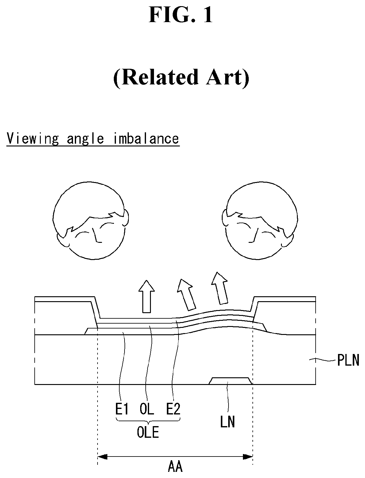
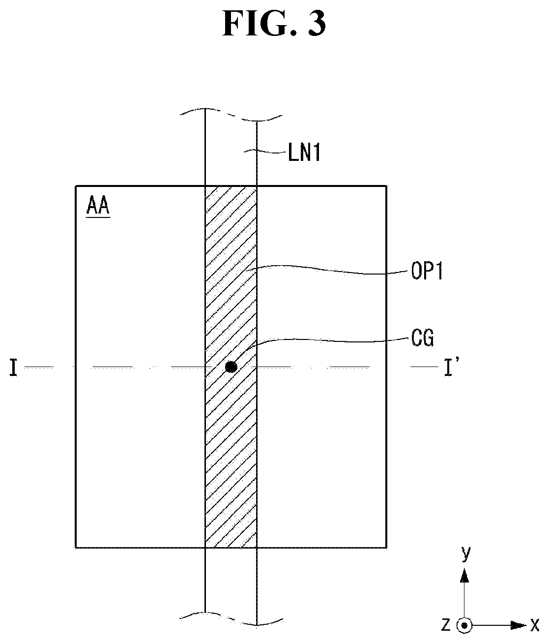
[0069]FIGS. 3 to 6 illustrate positional relationship between a light emitting area and a first wiring in an electroluminescent display according to a first embodiment of the present disclosure. FIG. 7 is a diagram for explaining an effect of the disclosure.
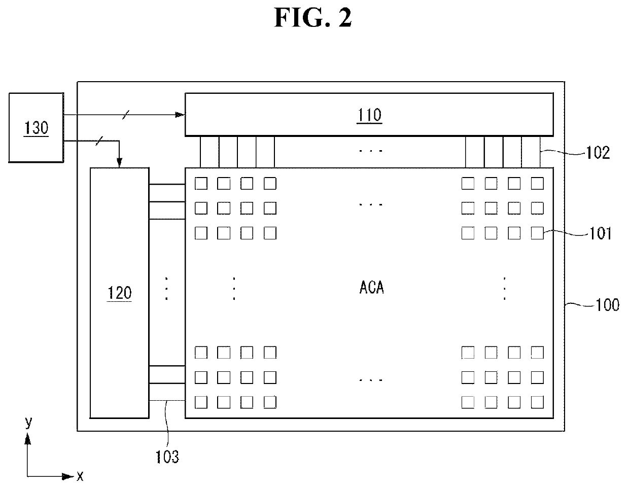
[0070]Referring to FIGS. 3 and 4, an electroluminescent display according to a first embodiment of the present disclosure includes a display panel having sub-pixels and wirings to which a signal (or a power supply voltage) for driving the sub-pixels is applied.
[0071]Each of the sub-pixels includes a transistor disposed on a substrate SUB and an organic light emitting diode OLE connected to the transistor. The organic light emitting diode OLE includes an anode E1 connected to the transistor, a cathode E2 disposed opposite the anode E1, and an organic light emitting layer OL interposed between the anode E1 and the cathode E2.
[0072]In each of the sub-pixels, a light emitting area AA having a predetermined planar shape is defined. Th...
second embodiment
[0082]FIGS. 8 to 11 illustrate positional relationship between a light emitting area and a first wiring in an electroluminescent display according to a second embodiment of the present disclosure.
[0083]Referring to FIGS. 8 and 9, an electroluminescent display according to a second embodiment of the present disclosure includes a display panel having sub-pixels and wirings to which a signal (or a power supply voltage) for driving the sub-pixels is applied.
[0084]Each of the sub-pixels includes a transistor disposed on a substrate SUB and an organic light emitting diode OLE connected to the transistor. The organic light emitting diode OLE includes an anode E1 connected to the transistor, a cathode E2 disposed opposite the anode E1, and an organic light emitting layer OL interposed between the anode E1 and the cathode E2.
[0085]In each of the sub-pixels, a light emitting area AA having a predetermined planar shape is defined. The planar shape of the light emitting area AA may be any one s...
third embodiment
[0098]FIGS. 12 and 13 illustrate positional relationship between a light emitting area and a second wiring in an electroluminescent display according to a third embodiment of the present disclosure. In the third embodiment, positional relationship between the light emitting area AA and a first wiring LN1 is substantially the same as that described in the first embodiment or the second embodiment.
[0099]Referring to FIG. 12, an electroluminescent display according to a third embodiment of the present disclosure includes a display panel having sub-pixels and wirings to which a signal (or a power supply voltage) for driving the sub-pixels is applied.
[0100]Each of the sub-pixels includes a transistor disposed on a substrate SUB and an organic light emitting diode OLE connected to the transistor. The organic light emitting diode OLE includes an anode E1 connected to the transistor, a cathode E2 disposed opposite the anode E1, and an organic light emitting layer OL interposed between the a...
PUM
| Property | Measurement | Unit |
|---|---|---|
| frequency | aaaaa | aaaaa |
| frequency | aaaaa | aaaaa |
| frequency | aaaaa | aaaaa |
Abstract
Description
Claims
Application Information
 - R&D
- Intellectual Property
- Life Sciences
- Materials
- Tech Scout
- Unparalleled Data Quality
- Higher Quality Content
- 60% Fewer Hallucinations
Browse by: Latest US Patents, China's latest patents, Technical Efficacy Thesaurus, Application Domain, Technology Topic, Popular Technical Reports.
© 2025 PatSnap. All rights reserved.Legal|Privacy policy|Modern Slavery Act Transparency Statement|Sitemap|About US| Contact US: help@patsnap.com