Memory device capable of performing high speed reading while realizing redundancy replacement

a memory device and redundancy replacement technology, applied in semiconductor devices, digital storage, instruments, etc., can solve the problems of high speed access, deterioration of access performance, and degradation of possible speed, so as to minimize fluctuations in the electric resistance of read current paths, improve the read margin and access time, and minimize imbalances in parasitic capacitance.

Inactive Publication Date: 2005-08-04
RENESAS ELECTRONICS CORP
View PDF3 Cites 1 Cited by
  • Summary
  • Abstract
  • Description
  • Claims
  • Application Information

AI Technical Summary

Benefits of technology

[0045] Therefore, a main advantage of the present invention is to minimize imbalances in parasitic capacitance between a plurality of read data buses to improve a read margin and an access time.
[0046] Another advantage of the present invention is to minimize fluctuations in electric resistance of read current paths in a case where data of a plurality of bits is simultaneously read, thereby enabling a read margin and an access time to be improved.
[0047] Still another advantage of the present invention is to enable a difference in electric resistance between a read current path for a normal memory cell and a read current path for a spare memory cell to be restricted to a small value, thereby enabling a read margin and an access time to be improved.
[0048] Yet another advantage of the present invention is to enable a difference in electric resistance between a read current path for a normal memory cell and a reference current path for a dummy memory cell to be restricted to a small value, thereby enabling a read margin and an access time to be improved.
[0049] Yet another advantage of the present invention is to enable an influence of electric resistance of a read current path to be reduced when simultaneous reading of a plurality of data because of separation of a plurality of read current paths from each others in a memory cell array.
[0050] Yet another advantage of the present invention is not only to realize a high speed access but also to generate a correct reference level by a simple and convenient dummy memory cells.

Problems solved by technology

Its possibility of a high speed access entails a problem of degradation of the possible speed, however, in a case where it has a redundancy architecture.
First, access performance becomes deteriorated in case of a large resistance value of a current path through which a read current of a selected memory cell flows, especially a large electric resistance of a source line of the memory cell.
Second, since in parallel access, simultaneous read operations are performed on a plurality of memory cells, a problem of an electric resistance of the source line becomes more conspicuous.

Method used


Image

  • Memory device capable of performing high speed reading while realizing redundancy replacement
  • Memory device capable of performing high speed reading while realizing redundancy replacement
  • Memory device capable of performing high speed reading while realizing redundancy replacement

Examples


first embodiment

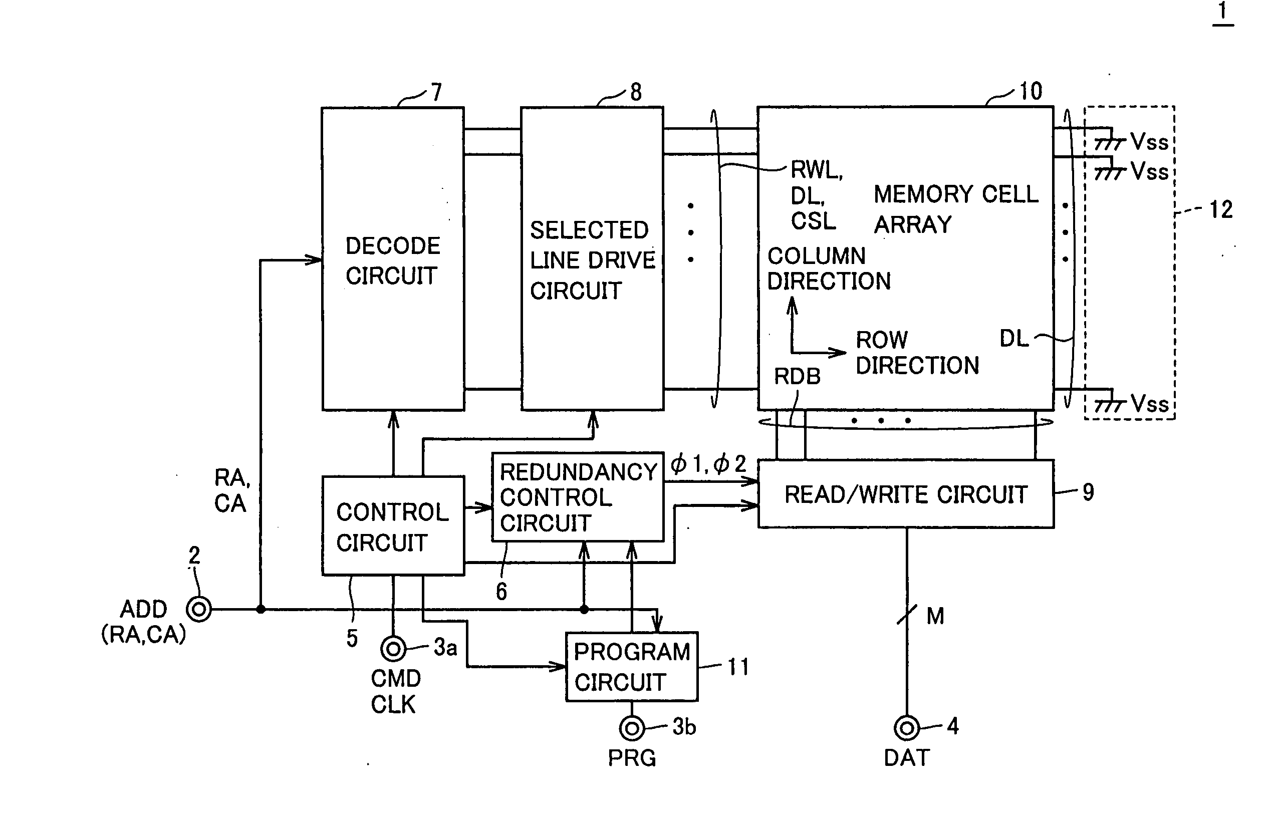
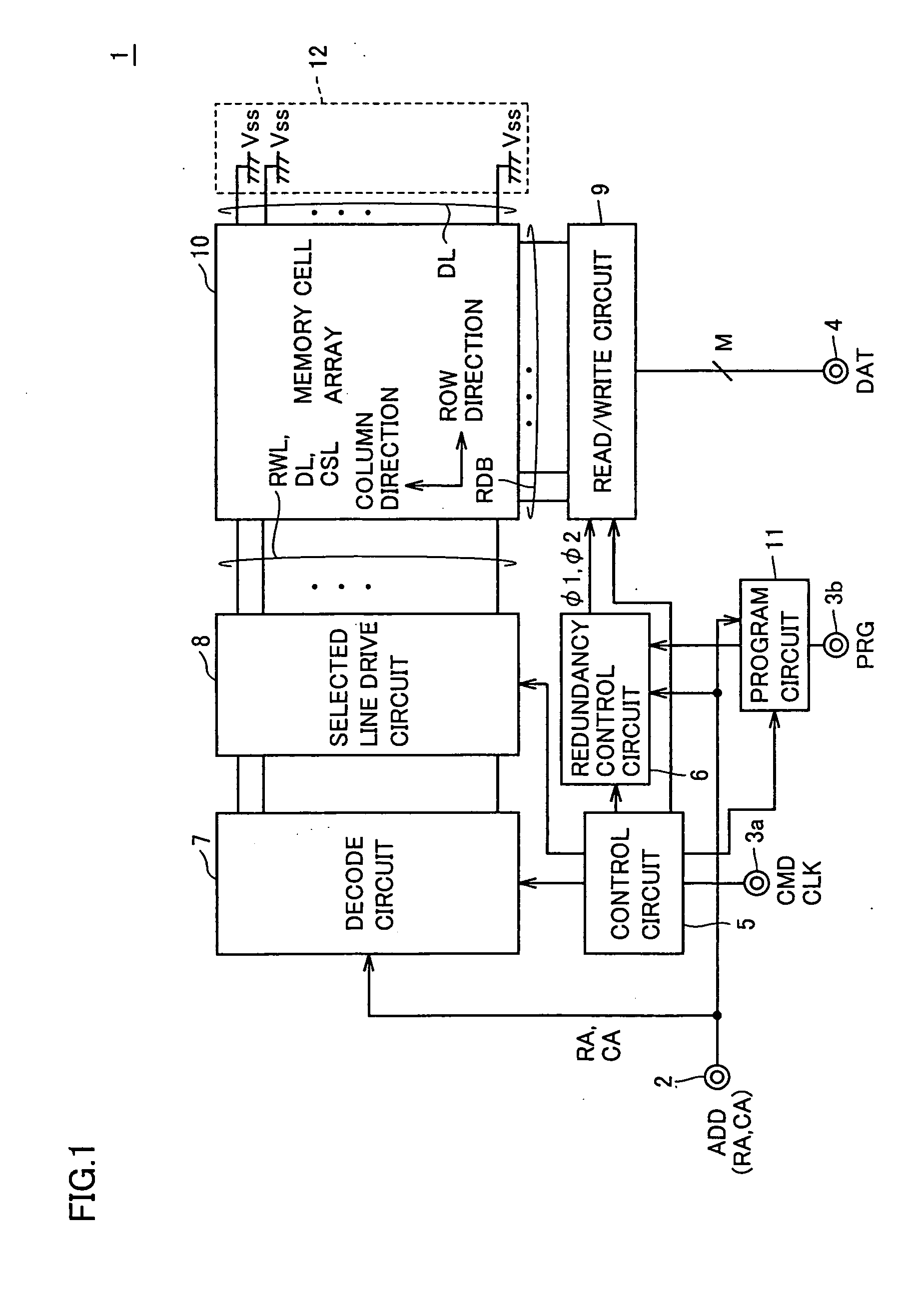
[0092]FIG. 1 is a schematic block diagram showing an overall architecture of an MRAM device 1 of a first embodiment of the present invention.

[0093] Referring to FIG. 1, MRAM device 1 performs supply / reception of a data signal DAT of M bits (wherein M is a natural number) according to a control signal CMD and an address signal ADD from outside. A data read operation and a data write operation in MRAM device 1 are performed at timings in synchronization with, for example, a clock signal CLK from outside. Alternatively, operation timings may be internally determined without receiving clock signal CLK from outside.

[0094] MRAM device 1 includes: an address terminal 2 receiving an input of address signal ADD; a signal terminal 3a receiving inputs of control signal CAD and clock signal CLK; a signal terminal 3b receiving an input of a program signal PRG activated in a program operation; and a data terminal 4 performing supply / reception of data signal DAT of M bits.

[0095] MR AM device 1 ...

second embodiment

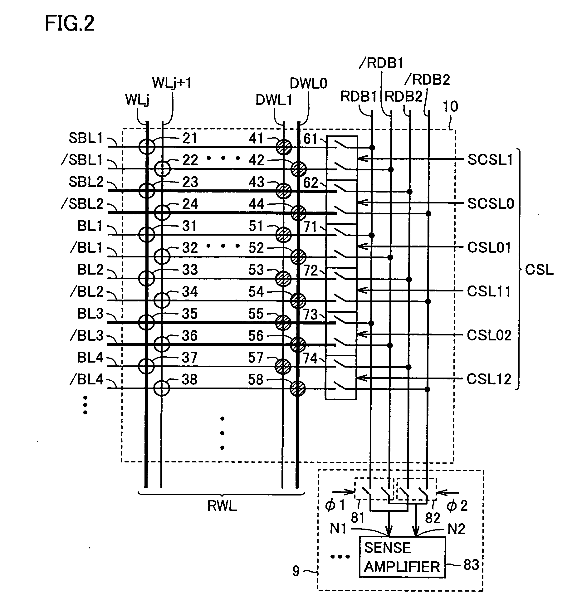
[0184] Description has been given of a case where simultaneous parallel access operations on a normal memory cell and a spare memory cell in the first embodiment. In this case, an imbalance occurs in read speed between memory cells if lengths of current paths along which read currents flow are different from each other according to locations of memory cells on which parallel accesses are made. If an imbalance in read speed occurs, an access time is limited by a memory cell with the slowest read speed; therefore, an access time is eventually deteriorated.

[0185]FIG. 16 is a circuit diagram showing a configuration of a memory cell array 310 used in a second embodiment. Note that the configuration shown in FIG. 16 is provided with a plurality of stages of sense amplifiers corresponding to the respective read data bus pairs as shown in FIG. 9 and effective in a case where read currents flow simultaneously through a plurality of read data buses.

[0186] While in FIG. 9, word lines and dum...

third embodiment

[0206] In the first embodiment, description has been given of a case where simultaneous accesses are made to a normal memory cell and a spare memory cell. At this time, there alises a problem that an accesses time is deteriorated by electric resistance of a superimposed portion, especially a common source line, of a plurality of read current paths accessed in parallel.

[0207] That is, when 2 currents flowing in a normal memory cell and a spare memory cell flow through the same source line, a float of a source potential is doubled to thereby delay a access time to be longer. In this case, it is only required to arrange source lines and word lines so as to separate a path of a current flowing in a normal memory cell and a path of a current flowing in a spare memory cell from each other at all times.

[0208]FIG. 22 is a circuit diagram showing a configuration of a memory cell array 610 used in a third embodiment in which a read current path is separated.

[0209] Referring to FIG. 22, mem...


PUM


Abstract

When normal bit lines BL3 and / BL3 are selected, spare bit lines SBL2 and / SBL2 are simultaneously selected, so that column select gates are placed in such a manner that these bit line pairs are connected to respective different read data bus pairs. The column select gates are distributed in placement so as not to cause a great difference in load capacitance between read data buses. A redundancy determination result is reflected on read data by activation of control signals φ1 and φ2 given immediately prior to a sense amplifier. Note that two sense amplifier may be provided with control signals φ1 and φ2 so as to select the outputs of one sense amplifier. With such a configuration adopted, it is possible to provide a memory device capable of performing high speed reading while realizing a redundancy replacement.

Description

[0001] This application is a continuation of application Ser. No. 10 / 651,841, filed on Jul. 10, 2003.BACKGROUND OF THE INVENTION [0002] 1. Field of the Invention [0003] The present invention relates to a memory device, and more particularly to a redundancy architecture capable of performing a high speed operation of a magnetic random access memory (MRAM). [0004] 2. Description of the Background Art [0005] An MRAM Magnetic Random Access Memory) device has received attention as a memory device capable of performing high speed non-volatile data storage. An MRAM device is a memory device using a plurality of thin film magnetic elements formed on a semiconductor integrated circuit to perform non-volatile data storage, and being capable of performing a random access to each of the thin film magnetic elements. [0006] It is reported that, especially in recent years, performance of an MRAM device has dramatically progressed by using thin film magnetic elements utilizing a magnetic tunnel jun...

Claims


Application Information

Patent Timeline
Patent Type & Authority Applications(United States)
IPC IPC(8): G11C11/15G11C5/00G11C7/00G11C7/12G11C11/00G11C11/16G11C29/00G11C29/04H01L21/8246H01L27/105H01L43/08
CPCG11C29/846G11C11/16
Inventor HIDAKA, HIDETO
Owner RENESAS ELECTRONICS CORP
Why Eureka
Try Eureka