
Longitudinal silicon ingot slicing machine and jig fixture

a long-range, silicon ingot technology, applied in metal sawing machines, stone-like material working apparatuses, crystal growth processes, etc., can solve the problems of large waste of space on each of the wafers, wasting space, and conventional methods

Active Publication Date: 2020-03-17
MESSINGER SAMUEL
View PDF4 Cites 3 Cited by
  • Summary
  • Abstract
  • Description
  • Claims
  • Application Information

AI Technical Summary

Benefits of technology

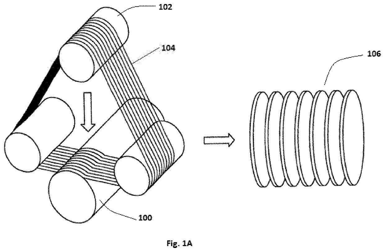
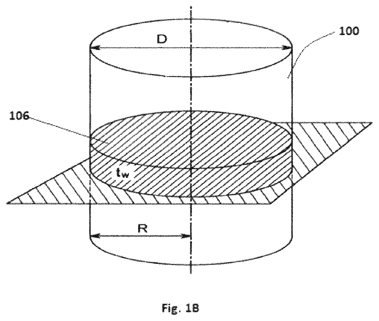
This patent is about a new method and system for making semiconductor wafers by cutting silicon ingots on their sides to produce rectangular wafers. This approach increases the area by 1.95 times than conventional methods using round wafers, resulting in a higher chip yield. Additionally, the method uses a novel wire machine apparatus and a novel JIG that guide and protect the diamond-embedded wires during slicing, and also release slurry and debris automatically. The new method and system have improved efficiency and yield compared to conventional methods.

Problems solved by technology

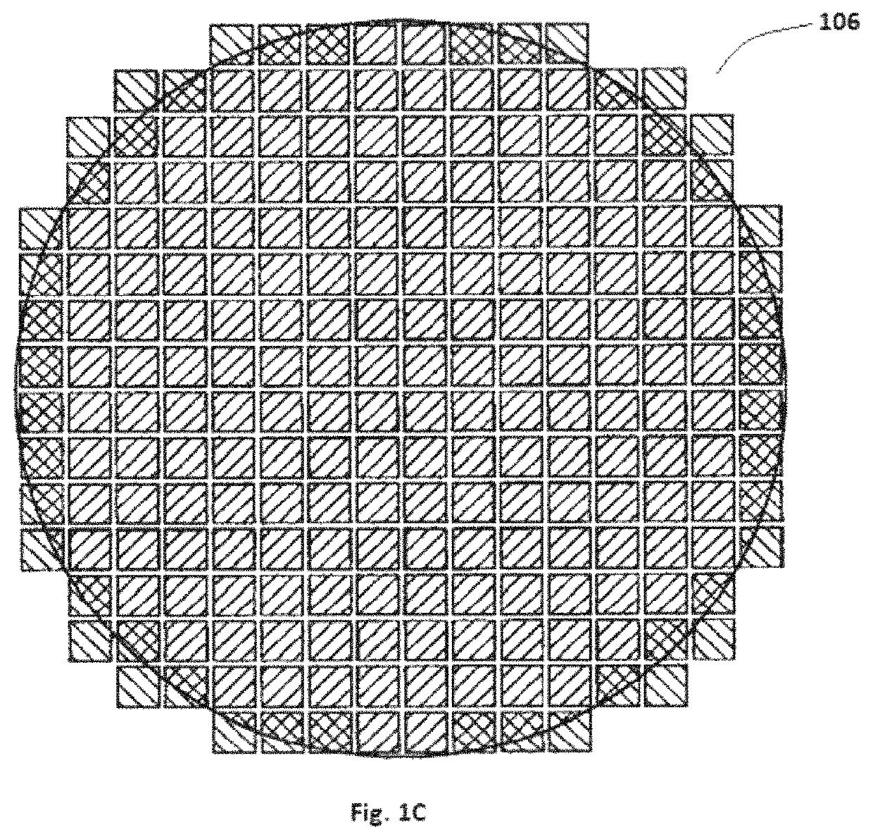
But this resulting circular wafers made from the conventional method has number of drawbacks such as waste of space due to conflict in geometry of fabricated chips on wafer and geometry of wafer itself.
Since, the chips are square in shape while wafers are circular in shape, there is lot of wasted space on each of wafers due to a conflict with geometry.
Other factors in addition to the waste due to geometry conflict are waste due to edge exclusion and polishing that further reduces the available wafer space for usable chips.

Method used


Image

  • Longitudinal silicon ingot slicing machine and jig fixture
  • Longitudinal silicon ingot slicing machine and jig fixture
  • Longitudinal silicon ingot slicing machine and jig fixture

Examples


Embodiment Construction

[0042]The embodiment herein and the various features and advantageous details thereof are explained more fully with reference to the non-limiting embodiments and detailed in the following description. Descriptions of well-known components and processing techniques are omitted so as to not unnecessarily obscure the embodiments herein. The examples used herein are intended merely to facilitate an understanding of ways in which the method and embodiments herein may be practiced and to further enable those of skill in the art to practice the embodiments herein. Accordingly, the examples should not be construed as limiting the scope of the embodiments herein.

[0043]According to an embodiment, the present invention discloses a novel method of longitudinal slicing of silicon ingot to maximize the chip yield where the longitudinal slicing refers to the longitudinal cutting of cylindrical silicon ingot along its longitudinal axis using any of the cutting apparatus of silicon ingot. Further, t...


PUM

PropertyMeasurementUnit
Fractionaaaaaaaaaa
Angleaaaaaaaaaa
Areaaaaaaaaaaa

Abstract

The present subject matter discloses a method of lateral slicing of cylindrical silicon ingot to maximize resulting chips yield as compared to the conventional transverse slicing of ingot. The resulting rectangular wafers made from lateral slicing of ingot maximizes yield as by the lateral slicing of ingot, overall chips per wafer ratio gets increased as compared to transversal cutting while the said method decreases waste due to conflict between chip and wafer geometry. The novel apparatus or system of present method includes JIG having plurality of parallel bars. The JIG is provided to covers and holds the ingot during slicing while the parallel bars of JIG between which diamond dust embedded wires gets located and which behaves as a guide for diamond embedded wires during the slicing of ingot. Also, this JIG mechanism protects and holds the wires from sliding down and miss the designated location of slicing during the process as the slicing of cylindrical ingot is being done longitudinally. Further, the parallel bars of the JIG mechanism are made such a way that the slurry and debris from the slicing automatically gets released.

Description

TECHNICAL FIELD[0001]The present invention relates to the field of preparation of semiconductor wafers from silicon ingot and maximizing overall chips per wafer. More specifically, it discloses a method of lateral slicing a silicon ingot diagonally for production of rectangular semiconductor wafers from cylindrical semiconductor ingot instead of circular wafers that increases overall chips per wafer ratio and decreases waste due to conflict between chip and wafer geometry compared to circular wafers.DESCRIPTION OF RELATED ART[0002]Conventionally, the silicon wafers which are used in fabrication of silicon chips are made by slicing circular wafers from cylindrical, purified silicon ingots, where ingots are sliced perpendicular to longitudinal axis of the silicon ingot resulting in a silicon wafers circular in shape. But this resulting circular wafers made from the conventional method has number of drawbacks such as waste of space due to conflict in geometry of fabricated chips on waf...

Claims


Application Information

Patent Timeline
IPC IPC(8): B28D5/00B28D5/04C30B29/06H01L21/304H01L21/02
CPCB28D5/045H01L21/02008C30B29/06H01L21/304B23D57/0061C30B33/06
Inventor MESSINGER, SAMUEL
Owner MESSINGER SAMUEL
Learn More