

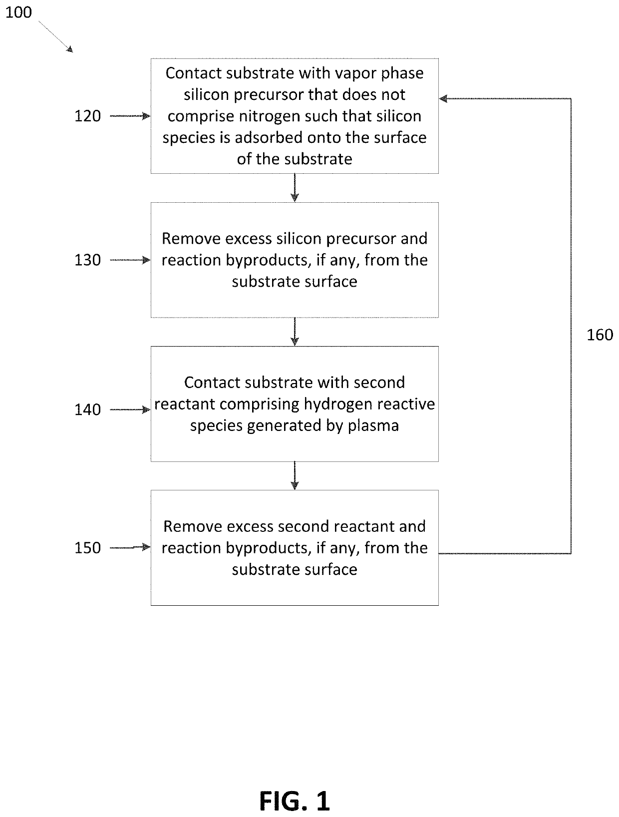
Formation of SiOC thin films
a technology of silicon oxycarbide and thin film, which is applied in the direction of coating, metallic material coating process, chemical vapor deposition coating, etc., can solve the problem of photoresist poisoning
- Summary
- Abstract
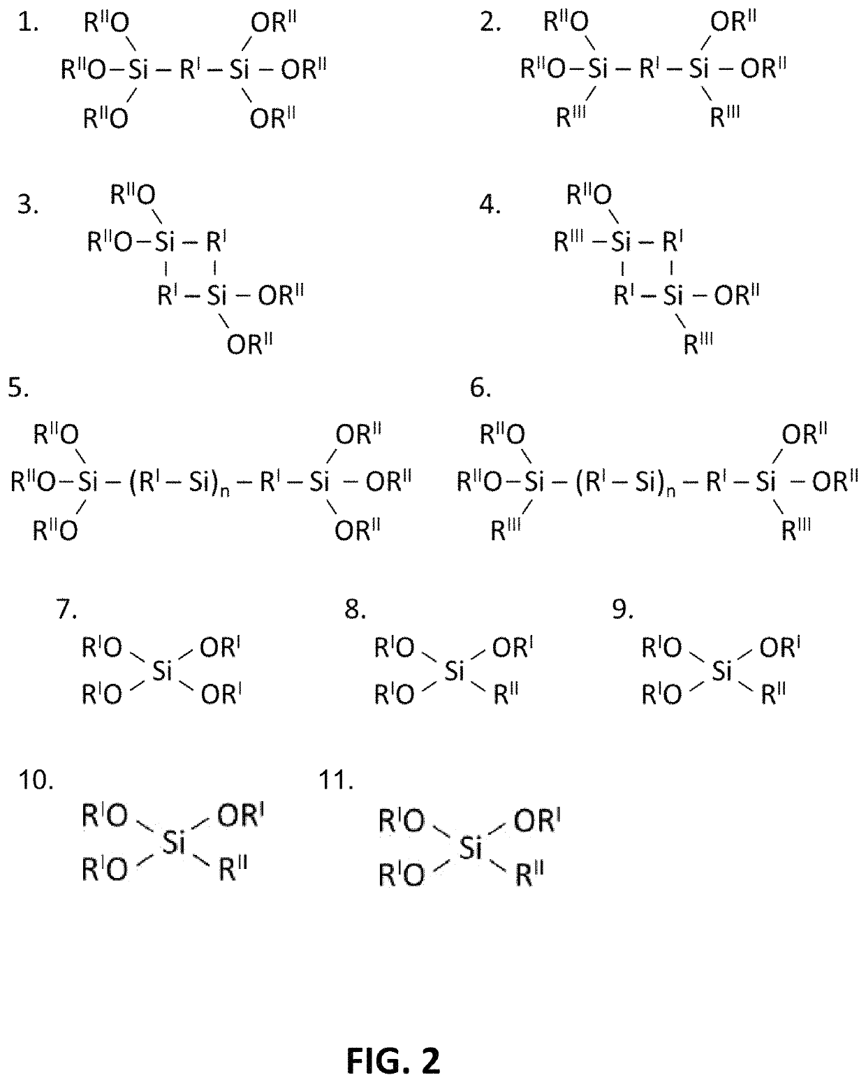
- Description
- Claims
- Application Information
AI Technical Summary
Benefits of technology
Problems solved by technology
Method used
Image

Examples
examples
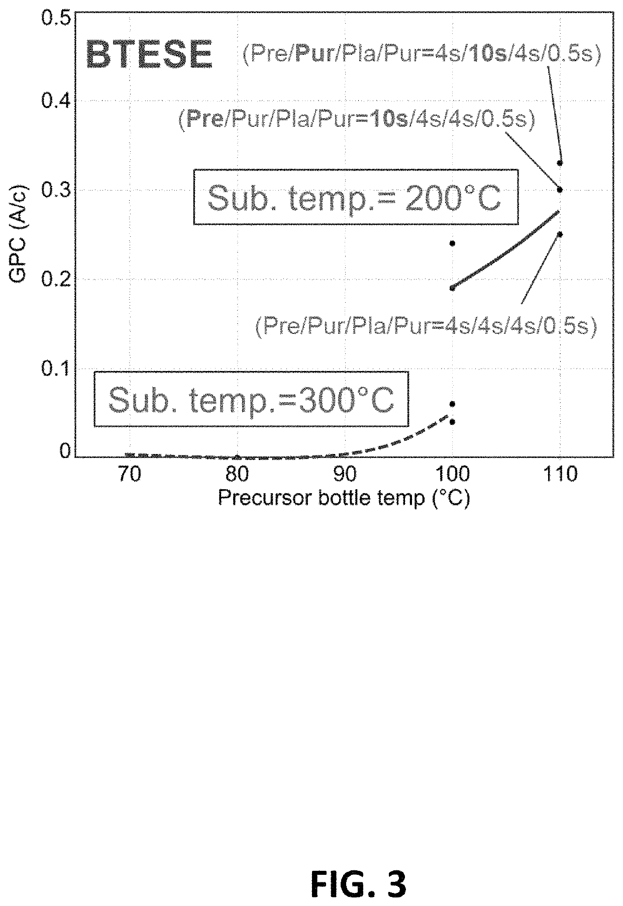
[0167]Exemplary SiOC thin films were deposited by a PEALD process as described herein. BTESE was used as a silicon precursor while the bottle temperature was varied from 80° C. to 110° C. H2 was used as the second reactant and a plasma was generated by applying 200 W of RF power to the second reactant. Certain SiOC samples were deposited using a substrate, or deposition temperature of 200° C., while other SiOC samples were depositing using a deposition temperature of 300° C.
[0168]For some SiOC samples, the precursor pulse time was 4 seconds, the precursor purge time was 4 seconds, the plasma pulse time was 4 seconds, and the plasma purge time was 0.5 seconds. For other samples the precursor pulse time was 10 seconds, the precursor purge time was 4 seconds, the plasma pulse time was 4 seconds, and the plasma purge time was 0.5 seconds. For other samples, the precursor pulse time was 4 seconds, the precursor purge time was 10 seconds, the plasma pulse time was 4 seconds, and the plasm...
PUM
| Property | Measurement | Unit |
|---|---|---|
| RF power | aaaaa | aaaaa |
| temperature | aaaaa | aaaaa |
| temperature | aaaaa | aaaaa |
Abstract
Description
Claims
Application Information