Method of measuring a target, and metrology apparatus

a target measurement and target technology, applied in the field of metrology, can solve problems such as reducing the robustness or reliability of overlay error measuremen

Active Publication Date: 2020-03-31
ASML NETHERLANDS BV
View PDF25 Cites 3 Cited by
  • Summary
  • Abstract
  • Description
  • Claims
  • Application Information

AI Technical Summary

Problems solved by technology

It has been found that changes in the manufacturing process of the semiconductor device can reduce the robustness or reliability of overlay error measurements.

Method used


Image

  • Method of measuring a target, and metrology apparatus
  • Method of measuring a target, and metrology apparatus
  • Method of measuring a target, and metrology apparatus

Examples


Embodiment Construction

[0088]Before describing embodiments of the invention in detail, it is instructive to present an example environment in which embodiments of the present invention may be implemented.

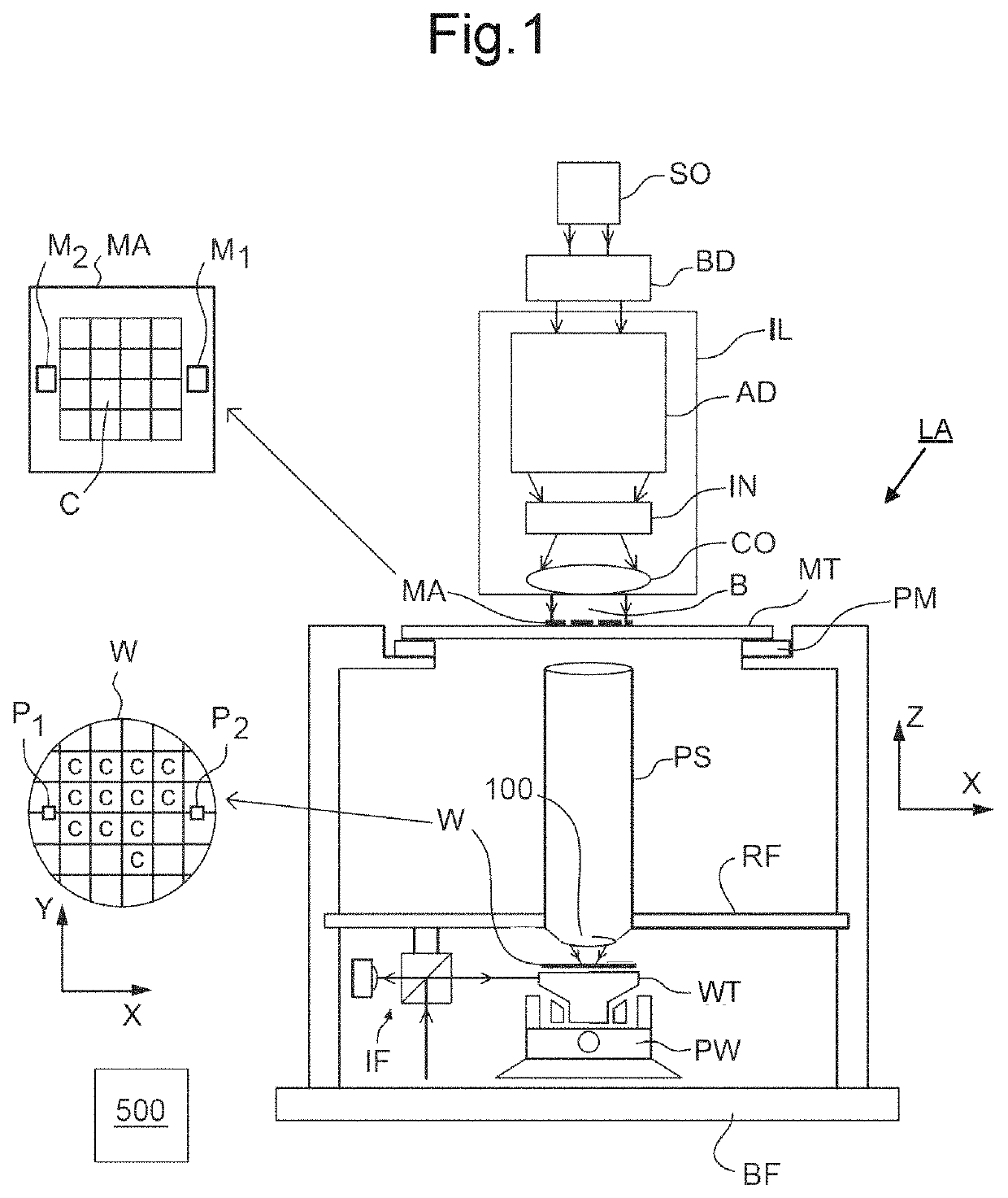
[0089]FIG. 1 schematically depicts a lithographic apparatus LA. The apparatus includes an illumination optical system (illuminator) IL configured to condition a radiation beam B (e.g., UV radiation or DUV radiation), a patterning device support or support structure (e.g., a mask table) MT constructed to support a patterning device (e.g., a mask) MA and connected to a first positioner PM configured to accurately position the patterning device in accordance with certain parameters; a substrate table (e.g., a wafer table) WT constructed to hold a substrate (e.g., a resist coated wafer) W and connected to a second positioner PW configured to accurately position the substrate in accordance with certain parameters; and a projection optical system (e.g., a refractive projection lens system) PS configured to proj...


PUM

PropertyMeasurementUnit
sizeaaaaaaaaaa
wavelengthaaaaaaaaaa

Abstract

Disclosed is a method of measuring a target, and a metrology apparatus. In one arrangement the target comprises a layered structure. The layered structure has a first target structure in a first layer and a second target structure in a second layer. The method comprises illuminating the target with measurement radiation using an illumination profile in the illumination pupil (u) that is offset from an imaginary line (IL) in the illumination pupil passing through the optical axis, to allow propagation to a detection region of the detection pupil of an allowed order (v2, v4) of a predetermined diffraction order while limiting propagation to the detection region of an equal and opposite order (v1′, v3′) of that predetermined diffraction order. Scattered radiation of plural double-diffracted allowed diffraction orders (w2, w4) is detected. A characteristic of the lithographic process is calculated using the detected scattered radiation of the predetermined diffraction orders.

Description

BACKGROUNDField of the Invention[0001]The present invention relates to methods and apparatus for metrology usable, for example, in the manufacture of devices by lithographic techniques.Background Art[0002]A lithographic apparatus is a machine that applies a desired pattern onto a substrate, usually onto a target portion of the substrate. A lithographic apparatus can be used, for example, in the manufacture of integrated circuits (ICs). In that instance, a patterning device, which is alternatively referred to as a mask or a reticle, may be used to generate a circuit pattern to be formed on an individual layer of the IC. This pattern can be transferred onto a target portion (e.g., including part of, one, or several dies) on a substrate (e.g., a silicon wafer). Transfer of the pattern is typically via imaging onto a layer of radiation-sensitive material (resist) provided on the substrate. In general, a single substrate will contain a network of adjacent target portions that are success...

Claims


Application Information

Patent Timeline
Patent Type & Authority Patents(United States)
IPC IPC(8): G03F7/20G03F9/00
CPCG03F7/70683G03F7/70625G03F9/7049G03F7/70158G03F7/7065G03F9/7003G03F7/70633
Inventor ZWIER, OLGER VICTOR
Owner ASML NETHERLANDS BV
Why Eureka
Try Eureka