Classification and localization of hotspots in integrated physical design layouts

a physical design and layout technology, applied in the field of integrated circuit design, can solve the problems of failure of fabricated devices, circuit design may not be manufacturable or inoperable in its first iteration, and become more difficult to ensure that the circuit design meets all practical manufacturability requirements, and achieves the effect of increasing the likelihood of a hotspo

Active Publication Date: 2020-04-14
INT BUSINESS MASCH CORP
View PDF8 Cites 5 Cited by
  • Summary
  • Abstract
  • Description
  • Claims
  • Application Information

AI Technical Summary

Problems solved by technology

As component sizes progressively decrease and as the complexity of integrated circuit designs increases, it becomes more difficult to guarantee that the circuit design meets all practical manufacturability requirements.
As a result, a circuit design may not be manufacturable or may be inoperable in its first iteration, necessitating extensive testing and iterative design revisions.
In particular, semiconductor manufacturing processes will often run into “hotspots,” which represent manufacturing errors such as, e.g., pinching, bridging, and missing patterns, which could lead to failure of fabricated devices.
Existing approaches to hotspot identification, such as process simulation and geometric verification, are each lacking in significant ways.
Such simulations are resource-intensive and time-consuming when evaluating larger layouts.
Furthermore, the accuracy of the resulting hotspot classification depends on the quality of the simulation, with hotspots potentially being missed if the simulation is lacking.
Pattern matching methods in particular are only useful for known hotspot configurations and are inadequate for identifying previously unknown hotspots.
In addition, both process simulation and geometric verification are generally limited to the detection of intra-layer hotspots that are confined to a single layer of physical design layout.
Inter-layer hotspots are even more computationally expensive to detect by process simulation and are nearly impossible to detect by geometric verification.

Method used


Image

  • Classification and localization of hotspots in integrated physical design layouts
  • Classification and localization of hotspots in integrated physical design layouts
  • Classification and localization of hotspots in integrated physical design layouts

Examples


Embodiment Construction

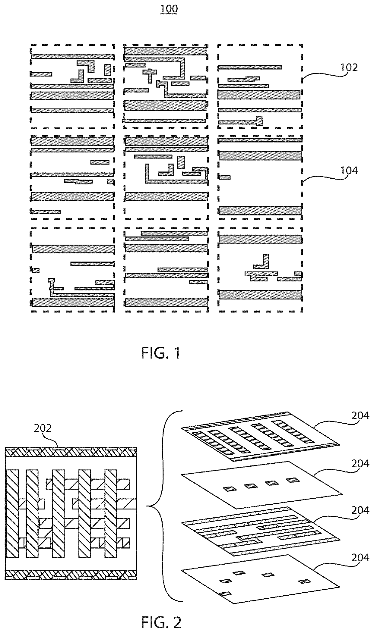
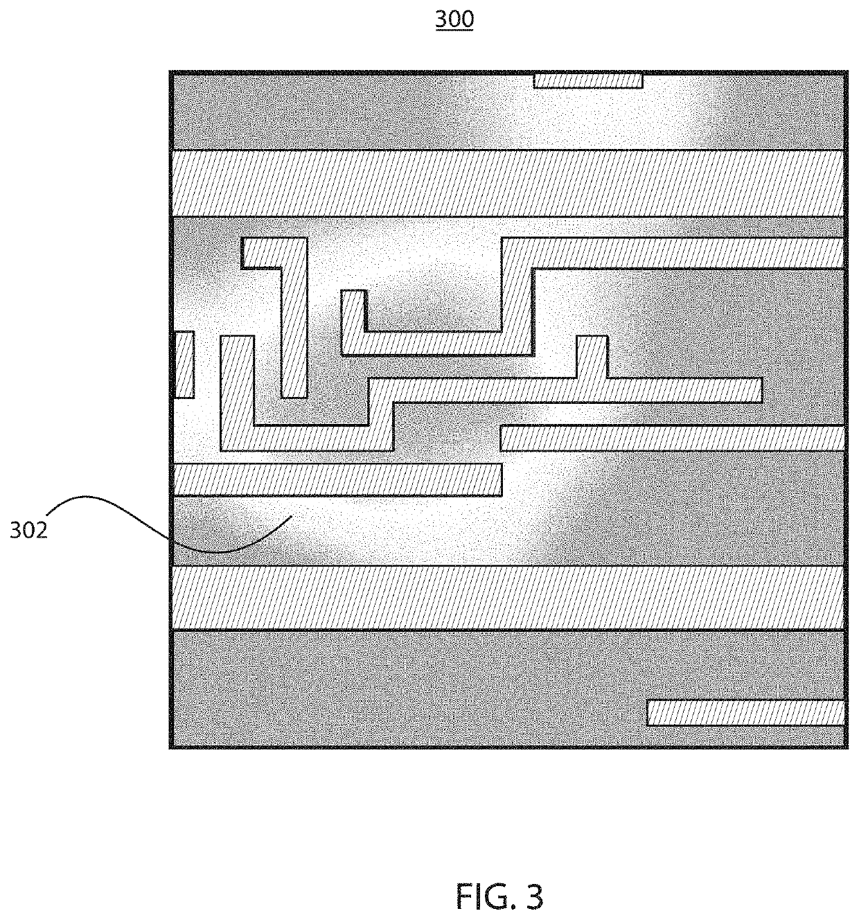
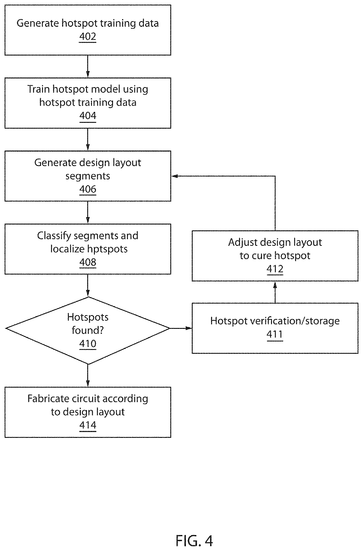
[0020]Embodiments of the present invention employ machine learning in the form of, e.g., deep neural networks, to automatically classify and localize hotspots in design layouts without simulation. A model is built based on training data of layout patterns and their labels to automatically extract features of hotspots from layouts and to localize which part of a given layout leads the model to its classification decision. The present embodiments thereby automatically and rapidly perform simultaneous classification and localization, detecting hotspots at any process step (e.g., including lithography and etch hotspots).

[0021]Toward that end, the present embodiments make use of training data that associates patterns of exemplary physical design layouts with a pre-determined classification of whether each pattern includes one or more hotspots. A deep convolutional neural network (CNN) may be used to build the model, though it should be understood that other forms of machine learning may ...


PUM

PropertyMeasurementUnit
heataaaaaaaaaa
areaaaaaaaaaaa
conductiveaaaaaaaaaa

Abstract

Methods and systems for fabricating an integrated circuit include training a machine learning model using a training set that includes known physical design layout patterns that are classified according to whether the patterns include a hotspot. It is determined whether an input physical design layout pattern includes a hotspot using the machine learning model. A hotspot localization is generated for the input physical design layout patterns. The input physical design pattern is adjusted to cure the hotspot. A circuit is fabricated in accordance with the adjusted input physical design layout pattern.

Description

BACKGROUNDTechnical Field[0001]The present invention generally relates to integrated circuit design and, more particularly, to fabricating integrated circuits that address potential hot spots using machine learning.Description of the Related Art[0002]As component sizes progressively decrease and as the complexity of integrated circuit designs increases, it becomes more difficult to guarantee that the circuit design meets all practical manufacturability requirements. As a result, a circuit design may not be manufacturable or may be inoperable in its first iteration, necessitating extensive testing and iterative design revisions. In particular, semiconductor manufacturing processes will often run into “hotspots,” which represent manufacturing errors such as, e.g., pinching, bridging, and missing patterns, which could lead to failure of fabricated devices. A hotspot does not necessarily identify a particular circuit component, but instead identifies a region of the design layout that i...

Claims


Application Information

Patent Timeline
Patent Type & Authority Patents(United States)
IPC IPC(8): G03F7/20
CPCG06F30/398G03F7/70433G06F2119/18G03F1/70G03F7/705G06F30/27G06F2119/08Y02P90/02
Inventor SHA, JINGSHAO, DONGBINGBURKHARDT, MARTINGUILLORN, MICHAEL A.
Owner INT BUSINESS MASCH CORP
Why Eureka
Try Eureka