Method of manufacturing 3-D semiconductor device

a semiconductor device and three-dimensional technology, applied in semiconductor devices, semiconductor/solid-state device details, electrical devices, etc., can solve the problems of increasing time consumption and manufacturing costs, difficult to perform multi-level cell operation, and increasing challenges in photoresist-slimming followed by stair-etching, so as to reduce the total number of etching process steps and improve the effect of area utilization of lead-out contact regions

Active Publication Date: 2020-04-28
INST OF MICROELECTRONICS CHINESE ACAD OF SCI
View PDF8 Cites 0 Cited by
  • Summary
  • Abstract
  • Description
  • Claims
  • Application Information

AI Technical Summary

Benefits of technology

[0025]In accordance with the manufacturing method of three-dimensional semiconductor device of the present invention, dividing the lead-out contact region into a plurality of sub-partitions and completing the multilayer film selective etching, performing the same process of photoresist-slimming and multilayer film etching in different sub-partitions, in order to selectively realize the selective etching for each sub-partition, thereby, the total number of etching process steps is reduced dramatically, and the area utilization of the lead-out contact region in three-dimensional devices is improved effectively.

Problems solved by technology

As the size of the memory cells of the two-dimensional (2D) memory devices continues to shrink, signal conflict and interference will significantly increase, so that it is difficult to perform operation of multi-level cell (MLC).
However, such circulating process of stepped photoresist-slimming followed by stair-etching is facing increasing challenges as the number of dielectric layers is increased, namely the multilayer laminated structures become thicken.
One factor is that each additional gate layer or insulating layer between gates correspondingly results in one more processing step for both photoresist-narrowing and stair-etching, so the time consumption and manufacturing cost grow up significantly due to the multiplication of processing steps.
And if the number of layers is too large, photoresist will be damaged severely, even some fracture or distortion can occur at the edge of the stairs, not only resulting in increased time consumption due to new photoresist re-coating, but also leading to short circuit or open circuit due to pattern distortion at the intermediate layer.
In addition, for each layer, the gate electrode is shared, therefore apart from one necessary lead-out contact hole, the rest area is wasted, which decreases the memory integration density.

Method used


Image

  • Method of manufacturing 3-D semiconductor device
  • Method of manufacturing 3-D semiconductor device
  • Method of manufacturing 3-D semiconductor device

Examples


Embodiment Construction

[0031]The features and technical effects of the present invention will be described in detail with reference to the drawings and schematic embodiments, disclosing a method for manufacturing a semiconductor device effectively improving the reliability of the device. It should be noted that the similar reference numbers denote the similar structure. The terms used in the present invention like “first”, “second”, “up / upon”, “down / low / beneath / under” etc. can be used in denoting various device structures, and do not indicate the relationship in space, sequence or hierarchy of the device structures unless specially illuminated these terms, if not stated otherwise.

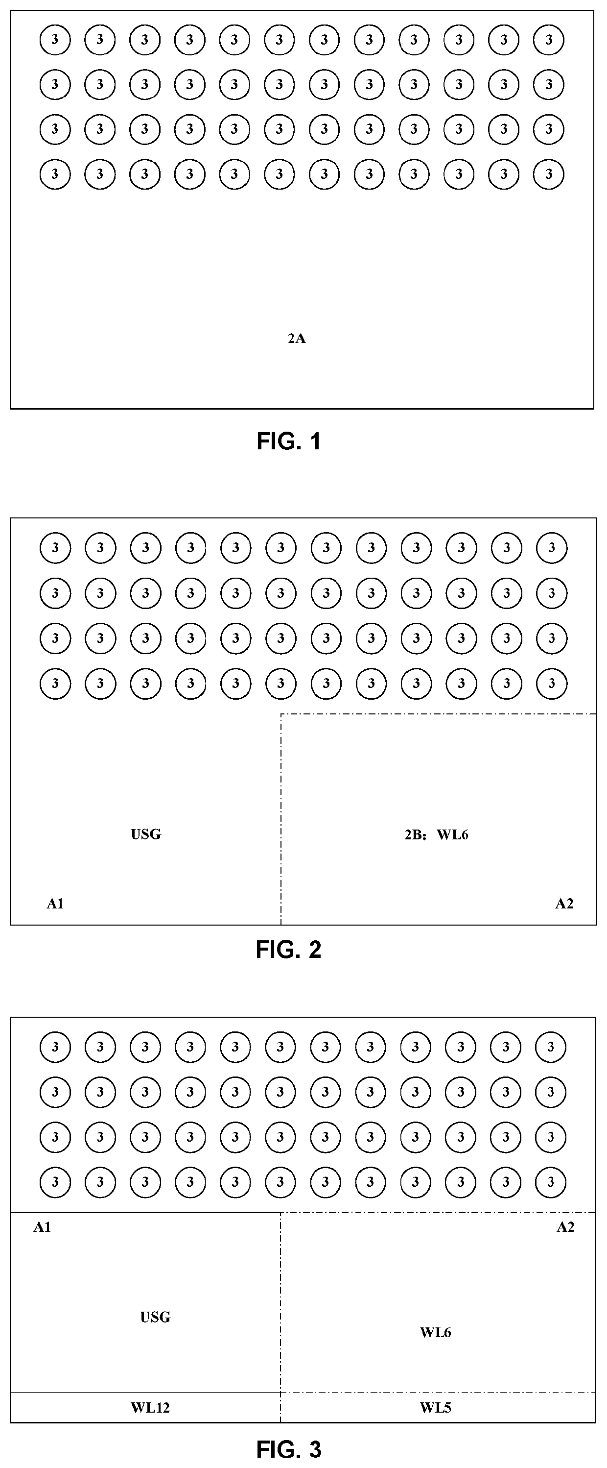
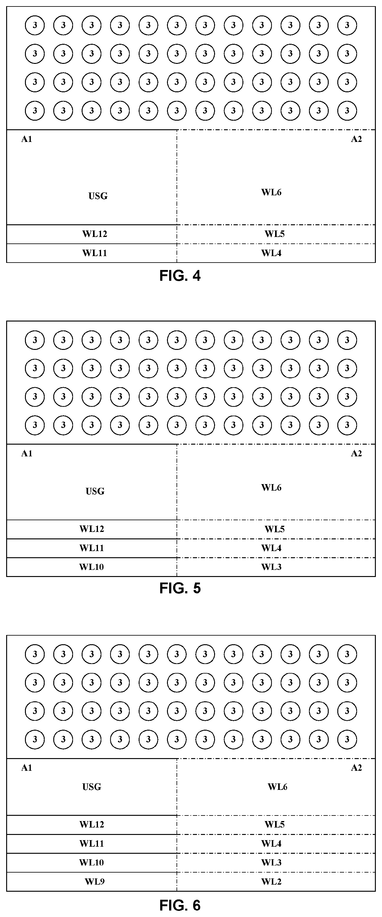
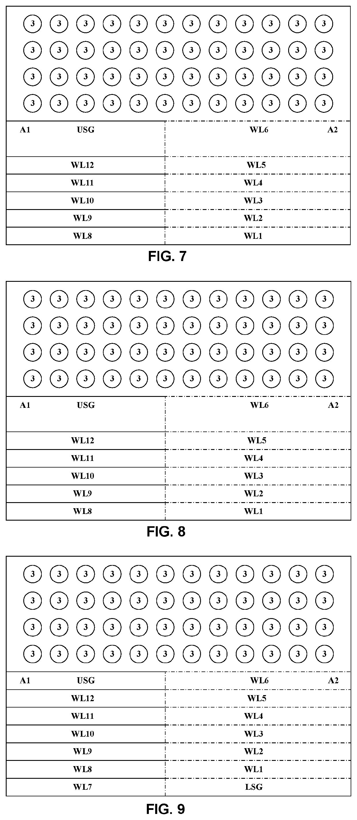
[0032]As shown in FIG. 1, the device unit is formed on the substrate 1. According to the embodiments shown in figures of the invention, the device units are a plurality of vertical channels 3. In other embodiments of the invention not shown in the figure, the device unit can be memory cells with floating gates made of polycrystal...


PUM

PropertyMeasurementUnit
heightaaaaaaaaaa
sizeaaaaaaaaaa
geometric shapesaaaaaaaaaa

Abstract

A method of manufacturing three-dimensional semiconductor device, comprising the steps of: a) forming a device unit on a substrate, the said device includes a plurality of stack structures composed of the first material layer and the second material layer stacked along a direction perpendicular to the substrate surface; b) forming a contact lead-out region around the said device unit, the contact lead-out region comprises a plurality of sub-partitions, each of the sub-partitions respectively exposes a different second material layer; c) forming a photoresist on said substrate, covering said plurality of sub-partitions, exposing a portion of said second material layer; d) using the photoresist as a mask, simultaneously etching the portion of the second material layer exposed by said plurality of sub-partitions, until another second material layer beneath said second material layer is exposed; e) slimming the size of the photoresist to expose a portion of said another second material layer; f) repeating said steps d and step e, until all of the second material layers are exposed; g) forming contact leads, connecting each of the plurality of the second material layers. In accordance with the method of the present invention, the total number of etching process steps is reduced dramatically and the area utilization is improved effectively by selectively etching each of the sub-partitions.

Description

[0001]This application is a National Phase application of, and claims priority to, PCT Application No. PCT / CN2014 / 081925, filed on Jul. 10, 2014, entitled “Method of Manufacturing 3-D Semiconductor Device”, which claimed priority to Chinese Application No. 201410174677.7, filed on Apr. 28, 2014. Both the PCT Application and Chinese Application are incorporated herein by reference in their entireties.TECHNICAL FIELD[0002]The present invention relates to a method of manufacturing semiconductor device, particularly to a method of manufacturing three-dimensional semiconductor device.BACKGROUND TECHNIQUE[0003]In order to improve the density of the memory device, the industry has worked extensively at developing a method for reducing the size of a two-dimensional arrangement of memory cells. As the size of the memory cells of the two-dimensional (2D) memory devices continues to shrink, signal conflict and interference will significantly increase, so that it is difficult to perform operati...

Claims


Application Information

Patent Timeline
Patent Type & Authority Patents(United States)
IPC IPC(8): H01L21/768H01L27/11565H01L27/11575H01L23/522H01L23/528H01L27/115H01L27/11519H01L45/00H01L27/11548H01L27/24H01L27/11556H01L27/11582
CPCH01L23/5226H01L27/11548H01L23/528H01L21/76816H01L27/11565H01L45/146H01L45/1675H01L27/115H01L27/11575H01L45/1226H01L45/145H01L27/11519H01L45/10H01L27/11582H01L27/2481H01L27/11556H10B63/80H10B41/20H10B63/84H10N70/25H10N70/823H10N70/883H10N70/8833H10N70/063H10B41/10H10B41/50H10B43/10H10B43/50H10B41/27H10B43/27H10B69/00
Inventor HUO, ZONGLIANG
Owner INST OF MICROELECTRONICS CHINESE ACAD OF SCI
Why Eureka
Try Eureka