Process of forming an electronic device including a transistor structure

a transistor and electronic device technology, applied in the direction of semiconductor devices, basic electric elements, electrical equipment, etc., can solve the problems of current collapse, carrier trapping, improved performance, and unfavorable dynamic on-state resistance,

Active Publication Date: 2020-05-05
SEMICON COMPONENTS IND LLC
View PDF13 Cites 4 Cited by
  • Summary
  • Abstract
  • Description
  • Claims
  • Application Information

AI Technical Summary

Benefits of technology

[0027]The process is well suited for a high mobility electron transistor (HEMT). In particular an unintentionally or very lightly doped channel layer may be capacitively coupled to a substrate and to the transistor terminals. The implant can help to create crystal defects in the channel and underlying layers that allow all of the channel layer within the transistor structure to be resistively coupled to the substrate and to the transistor terminals. The resistive coupling helps to prevent or substantially reduce the amount of charge accumulation that may occur within the channel region when in the off-state, particularly after the transistor structure has reached steady state. When the transistor structure is turned on after being at steady state in the off-state, the drain current quickly reaches steady state significantly faster than if the same transistor structure was not implanted or if only portions, and not substantially all, of the channel layer is implanted. Thus, dynamic on-state resistance is significantly improved.
[0026]An electronic device can include a transistor structure. A process of forming the electronic device can include providing a workpiece including a substrate, a first layer, and a channel layer including a compound semiconductor material. In an embodiment, the first layer can be any of a nucleation layer, a stress relief layer, an intermediate layer, or any combination thereof. The process can also include implanting a species into the workpiece such that the projected range extends at least into the channel and first layers, and the implant is performed into an area corresponding to at least a source region of the transistor structure. In an embodiment, the area corresponds to all or substantially all of the area occupied of the transistor structure.

Problems solved by technology

A problem with HEMTs is that they can suffer from current collapse, carrier trapping, and the like.
Improved performance, including improved dynamic on-state resistance, is undesired.

Method used


Image

  • Process of forming an electronic device including a transistor structure
  • Process of forming an electronic device including a transistor structure
  • Process of forming an electronic device including a transistor structure

Examples


embodiment 1

[0074] An electronic device can include a transistor structure. A process of forming the electronic device can include providing a workpiece including a substrate, a first layer, and a channel layer including a compound semiconductor material; and implanting a species into the workpiece such that the projected range extends at least into the channel and first layers, and the implant is performed into an area corresponding to at least a source region of the transistor structure.

[0075]Embodiment 2. The process of Embodiment 1, wherein implanting the species is performed such that the area corresponds to all or substantially all area occupied of the transistor structure.

[0076]Embodiment 3. The process of Embodiment 1, wherein the workpiece is not exposed to a thermal cycle at most 750° C. after implanting the species.

[0077]Embodiment 4. The process of Embodiment 3, wherein implanting the species is performed such that the species includes H+ ions.

[0078]Embodiment 5. The process of Embo...

embodiment 19

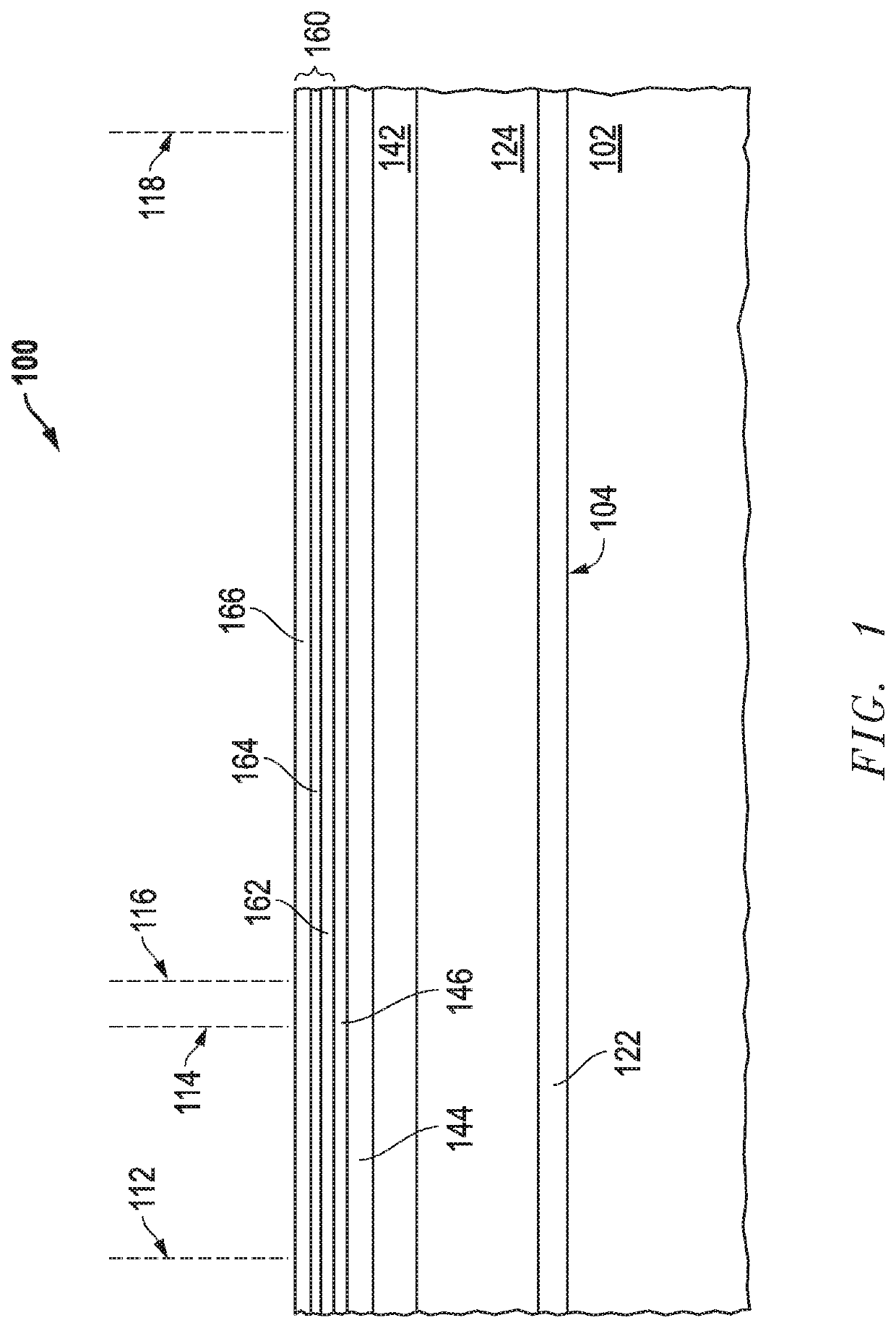
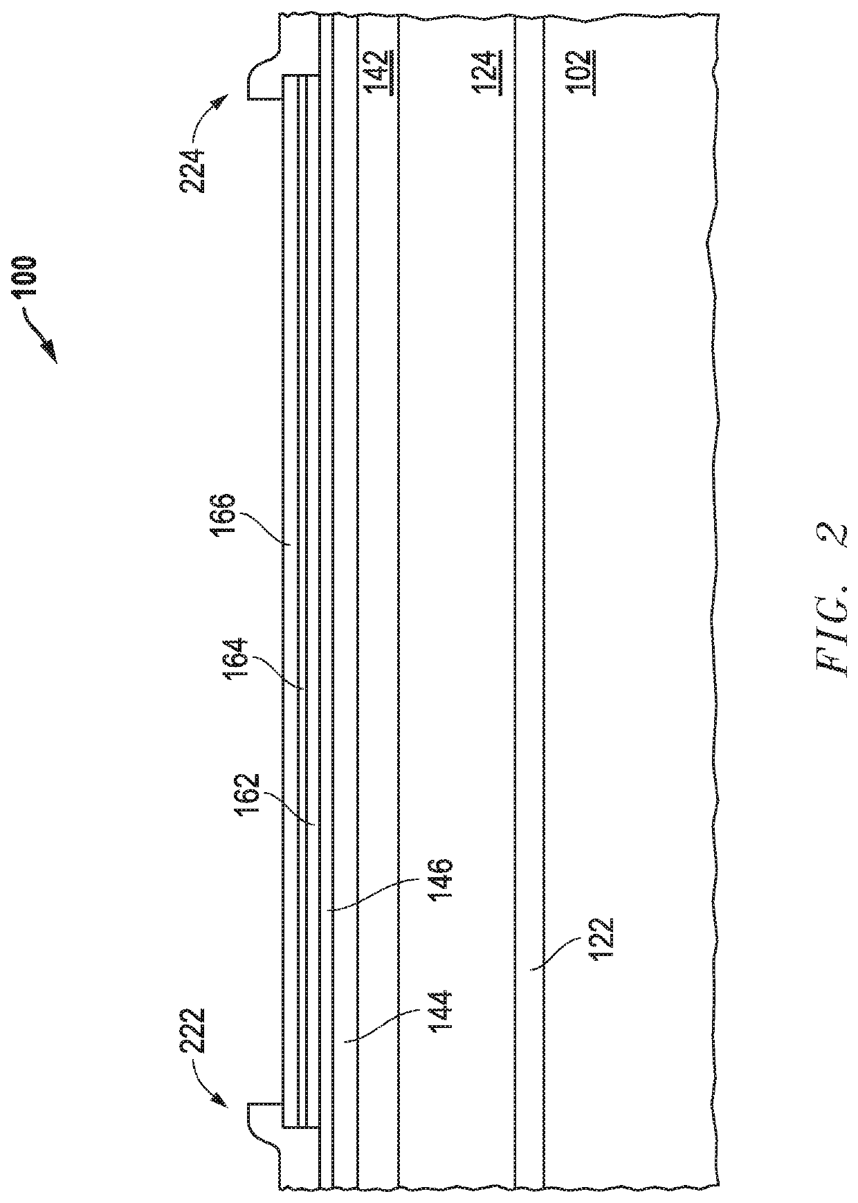
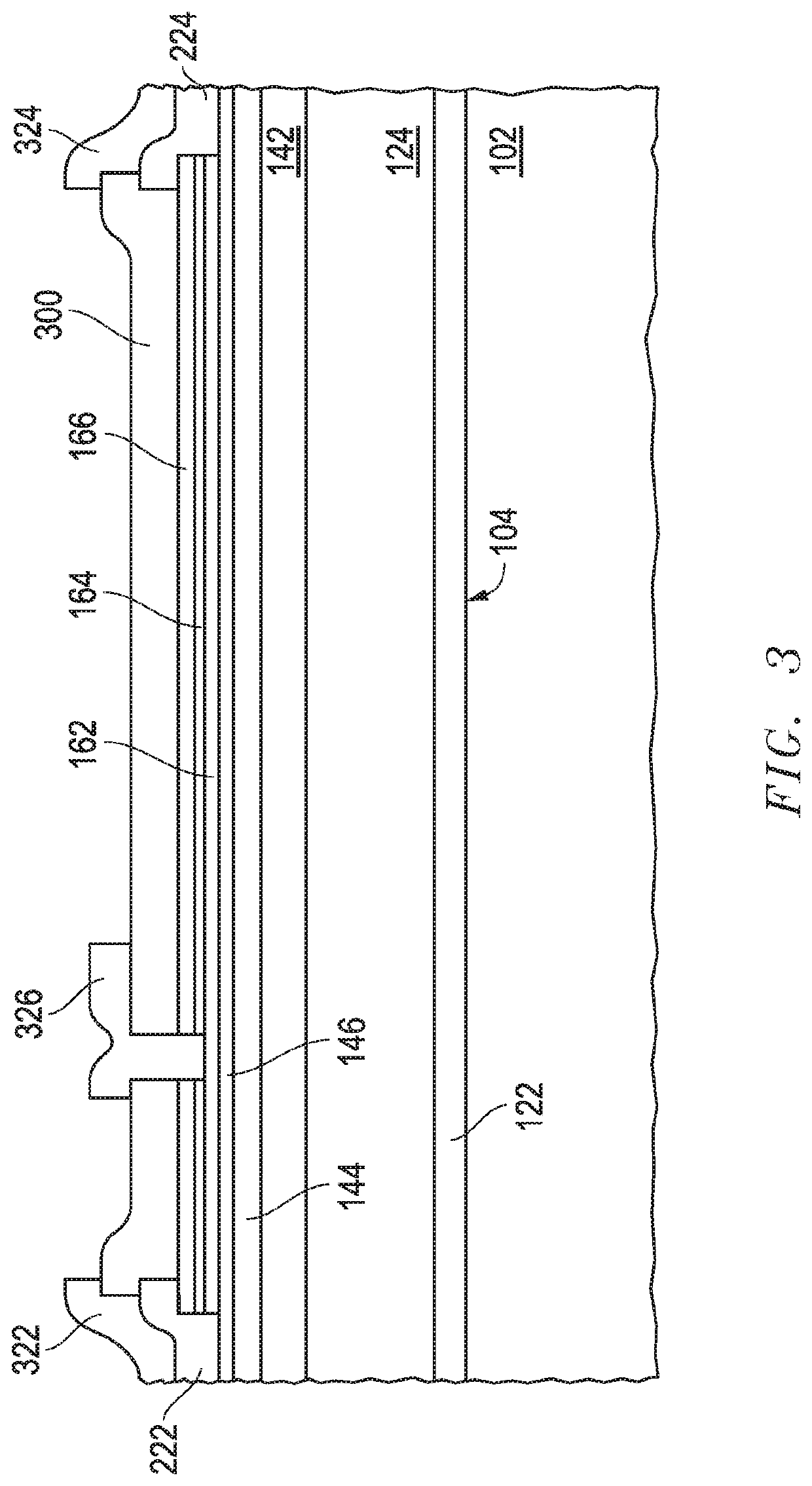
[0092] An electronic device can include a HEMT structure. A process of forming the electronic device can include providing a workpiece that includes a substrate; a first layer overlying the substrate, wherein a particular layer within the first layer is carbon doped at concentration of at least 1×10¹⁶ atoms / cm3; an intermediate layer overlying the first layer, wherein the intermediate layer includes Al(1-x)GaxN, where 016 atoms / cm3; a channel layer overlying the intermediate layer, wherein the channel layer includes GaN and is carbon doped at a concentration less than the intermediate layer; and a barrier layer overlying the channel layer, wherein the barrier layer includes In(1-a-b)AlaGabN, where 0≤a≤1, 0≤b≤1. The process can further include forming a source electrode and a drain electrode, wherein the source and drain electrodes contact to the barrier layer; forming a gate electrode overlying the barrier layer and between the source and drain electrodes; and implanting a species i...


PUM

PropertyMeasurementUnit
energyaaaaaaaaaa
energyaaaaaaaaaa
tilt angleaaaaaaaaaa

Abstract

An electronic device including a transistor structure, and a process of forming the electronic device can include providing a workpiece including a substrate, a first layer, and a channel layer including a compound semiconductor material; and implanting a species into the workpiece such that the projected range extends at least into the channel and first layers, and the implant is performed into an area corresponding to at least a source region of the transistor structure. In an embodiment, the area corresponds to substantially all area occupied by the transistor structure. In another embodiment, the implant can form crystal defects within layers between the substrate and source, gate, and drain electrodes. The crystal defects may allow resistive coupling between the substrate and the channel structure within the transistor structure. The resistive coupling allows for better dynamic on-state resistance and potentially other electrical properties.

Description

FIELD OF THE DISCLOSURE[0001]The present disclosure relates to electronic devices including transistor structures, and more particularly to, processes of forming electronic devices including transistor structures.RELATED ART[0002]High electron mobility transistors (HEMTs) can be used for high power applications. A problem with HEMTs is that they can suffer from current collapse, carrier trapping, and the like. Improved performance, including improved dynamic on-state resistance, is undesired.BRIEF DESCRIPTION OF THE DRAWINGS[0003]Embodiments are illustrated by way of example and are not limited in the accompanying figures.[0004]FIG. 1 includes an illustration of a cross-sectional view of a portion of a workpiece including a substrate, a nucleation layer, a stress relief layer, an intermediate layer, a channel layer, and an insulating layer.[0005]FIG. 2 includes an illustration of a cross-sectional view of the workpiece of FIG. 1 after patterning the insulating layer and forming sour...

Claims


Application Information

Patent Timeline
Patent Type & Authority Patents(United States)
IPC IPC(8): H01L21/265H01L29/40H01L29/778H01L29/32H01L29/66H01L29/20H01L21/324H01L21/266
CPCH01L29/66462H01L29/32H01L29/7786H01L29/7787H01L21/3245H01L21/2654H01L29/404H01L21/266H01L29/2003H01L29/778
Inventor MOENS, PETERBANERJEE, ABHISHEK
Owner SEMICON COMPONENTS IND LLC
Why Eureka
Try Eureka