Low capacitance and high-holding-voltage transient-voltage-suppressor (TVS) device for electro-static-discharge (ESD) protection

a transient voltage suppressor and low capacitance technology, applied in semiconductor devices, diodes, transistors, etc., can solve problems such as esd failures, low yield, and many different kinds of integrated circuits (ic's) that are prone to damage and failur

Active Publication Date: 2020-05-26
HONG KONG APPLIED SCI & TECH RES INST
View PDF16 Cites 2 Cited by
  • Summary
  • Abstract
  • Description
  • Claims
  • Application Information

AI Technical Summary

Problems solved by technology

Many different kinds of Integrated circuits (IC's) are prone to damage and failure from an electro-static-discharge (ESD) pulse.
ESD failures that occur in the factory contribute to lower yields.
ESD failures may also occur in the field when an end-user touches a device.
These smaller transistors are much more susceptible to over-voltage failure but can operate with a lower power-supply voltage, thus consuming less power and producing less heat.
Static charges from a person or machinery can produce such damaging currents that are only partially blocked by the input-protection circuits in the periphery.
Large size devices are expensive and undesirable.
Some prior-art ESD-protection devices are not suited for standard CMOS processes, such as ESD-protection devices that use insulator layers in Silicon-On-Insulator (SOI) processes.
Diodes have been uses as ESD-protection structures, but the diode's I-V characteristics allow for high voltages when large ESD currents flow, and these high voltages can still damage core transistors.
Some ESD-protection structures use two diodes in series rather than one diode, but such stacked diodes are undesirable in some environments due to the increased voltage drop of two diodes in series.
However, simply having a diode and an SCR in an ESD-protection structure may produce erratic results that depend on the relative locations of the SCR and diode and other structures such as guard rings.
Thermal failure can occur when breakdown voltage VBD is exceeded for too long of a period of time.
Thus the safe design window may shift and shrink.
The relatively low doping of N-well 62 can produce a low holding voltage, which can violate the safe design window.
Such a large capacitance is undesirable since it slows down normal signaling.
A Transient Voltage Suppressor (TVS) for ESD protection manufactured with a standard complementary metal-oxide-semiconductor (CMOS) process may have too much capacitance when large wells are incorporated into the TVS device.

Method used


Image

  • Low capacitance and high-holding-voltage transient-voltage-suppressor (TVS) device for electro-static-discharge (ESD) protection
  • Low capacitance and high-holding-voltage transient-voltage-suppressor (TVS) device for electro-static-discharge (ESD) protection
  • Low capacitance and high-holding-voltage transient-voltage-suppressor (TVS) device for electro-static-discharge (ESD) protection

Examples


Embodiment Construction

[0038]The present invention relates to an improvement in ESD-protection devices. The following description is presented to enable one of ordinary skill in the art to make and use the invention as provided in the context of a particular application and its requirements. Various modifications to the preferred embodiment will be apparent to those with skill in the art, and the general principles defined herein may be applied to other embodiments. Therefore, the present invention is not intended to be limited to the particular embodiments shown and described, but is to be accorded the widest scope consistent with the principles and novel features herein disclosed.

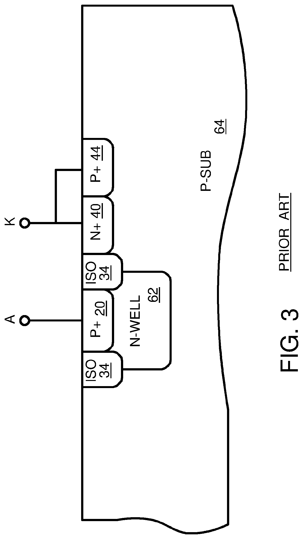
[0039]The inventors have recognized that the N-well in the SCR structure is relatively large in area and this large area increases capacitance. Removing the large N-well has the potential to significantly reduce capacitance.

[0040]FIG. 4 is a cross-sectional diagram of Transient Voltage Suppressor (TVS) SCR without an N-well. N+...


PUM

PropertyMeasurementUnit
voltageaaaaaaaaaa
voltageaaaaaaaaaa
thicknessaaaaaaaaaa

Abstract

A well-less Transient Voltage Suppressor (TVS) Silicon-Controlled Rectifier (SCR) has a P+ anode region that is not in an N-well. The P+ anode region 20 is surrounded by N+ isolation regions near the surface, and a deep N+ region underneath that is formed in a p-substrate. A N+ cathode region is formed in the p-substrate. The deep N+ region has a doping of 5×10¹⁸ to 5×10¹⁹ / cm3, compared to a doping of 1×10¹⁶ / cm3 for a typical N-well, or a doping of 1×10¹³ to 1×10¹⁵ / cm3 for the p-substrate. The high doping in the deep N+ region causes a recombination current that can shunt half of the anode current. Since the deep N+ region is much shallower than an N-well, the sidewall capacitance is greatly reduced, allowing for higher speed applications.

Description

FIELD OF THE INVENTION[0001]This invention relates to Electro-Static-Discharge (ESD) protection devices, and more particularly to a low-capacitance and high-holding voltage diode.BACKGROUND OF THE INVENTION[0002]Many different kinds of Integrated circuits (IC's) are prone to damage and failure from an electro-static-discharge (ESD) pulse. ESD failures that occur in the factory contribute to lower yields. ESD failures may also occur in the field when an end-user touches a device.[0003]Various ESD-protection structures have been placed near input, output, or bi-directional I / O pins of ICs. Many of these protection structures use passive components such as series resistors, diodes, and thick-oxide transistors. Other ESD structures use an active transistor to safely shunt ESD current.[0004]As manufacturing ability improves and device sizes shrink, lower voltages are applied to transistors during normal operation. These smaller transistors are much more susceptible to over-voltage failur...

Claims


Application Information

Patent Timeline
Patent Type & Authority Patents(United States)
IPC IPC(8): H01L27/02H01L29/08H01L29/74
CPCH01L29/7412H01L29/083H01L27/0262H01L29/402H01L29/87
Inventor MA, CHENYUEYAM, CHUN-KITHUO, XIAO
Owner HONG KONG APPLIED SCI & TECH RES INST
Why Eureka
Try Eureka