Semiconductor device and manufacturing method thereof

a semiconductor device and manufacturing method technology, applied in semiconductor devices, diodes, electrical apparatus, etc., can solve the problems of capacitance without voltage dependence, degradation in quality, and difficulty in using capacitance with voltage dependence, so as to reduce the voltage dependence of capacitance, and increase the manufacturing process

Active Publication Date: 2020-07-14
SEIKO EPSON CORP
View PDF9 Cites 0 Cited by
  • Summary
  • Abstract
  • Description
  • Claims
  • Application Information

AI Technical Summary

Benefits of technology

[0011]A first aspect of the invention relates to providing a semiconductor device in which a zener diode having a desired breakdown voltage and a capacitor in which voltage dependence of capacitance is reduced are mounted together in order to realize various circuits. Also, a second aspect of the invention relates to providing a method of manufacturing a semiconductor device in which a zener diode having a desired breakdown voltage and a capacitor in which voltage dependence of capacitance is reduced are mounted together without significantly increasing the manufacturing processes.
[0014]In this way, according to the first aspect of the invention, the vertical zener diode including the first impurity diffusion region that mainly determines the breakdown voltage and the capacitor including the second impurity diffusion region that reduces voltage dependence of capacitance are mounted together in the same semiconductor device, and thus various circuits can be realized.
[0015]The semiconductor device may further include at least one other well that is arranged so as to surround the second impurity diffusion region in the semiconductor layer. For example, as a result of providing a second conductivity type second well that surrounds the second impurity diffusion region and a first conductivity type third well that surrounds the second well in the semiconductor layer, the insulation properties of the first electrode of the capacitor can be improved.
[0016]Also, the semiconductor device may further include a second conductivity type semiconductor substrate in which the semiconductor layer is arranged; a first conductivity type buried diffusion layer that is arranged in the semiconductor substrate; and a first conductivity type fourth impurity diffusion region that is arranged in the semiconductor layer and surrounds the first region of the semiconductor layer on the buried diffusion layer in plan view. The buried diffusion layer and the fourth impurity diffusion region constitute a portion of a cathode region or an anode region of the vertical zener diode, and can improve the element isolation properties.
[0019]In this way, according to the second aspect of the invention, the first impurity diffusion region that mainly determines the breakdown voltage of the vertical zener diode and the second impurity diffusion region that reduces the voltage dependence of capacitance of the capacitor can be formed in the same processes and with the same conditions. Accordingly, a semiconductor device in which a zener diode having a desired breakdown voltage and a capacitor in which voltage dependence of capacitance is reduced are mounted together without significantly increasing the manufacturing processes.

Problems solved by technology

In circuit design, in general, a capacitance having voltage dependence is difficult to use, and a capacitance having no voltage dependence is desired.
However, if the impurity concentration in the electrode region is too high, degradation in quality occurs such as a reduction in capacitance of the MOS capacitor and a reduction in breakdown voltage of the gate insulating film caused by abnormal growth of an oxide film when the gate insulating film is formed by oxidizing a surface of the semiconductor substrate.
Meanwhile, when an attempt is made to mount a plurality of different types of circuit elements together in the semiconductor device, processes for forming dedicated impurity diffusion regions for respective circuit elements increase, and the manufacturing cost of the semiconductor device increases due to the increased number of masks and processes.

Method used


Image

  • Semiconductor device and manufacturing method thereof
  • Semiconductor device and manufacturing method thereof
  • Semiconductor device and manufacturing method thereof

Examples


Embodiment Construction

[0030]Hereinafter, an embodiment of the invention will be described in detail, with reference to the drawings. Note that the same constituent elements are given the same reference numerals, and a redundant description is omitted.

[0031]Semiconductor Device

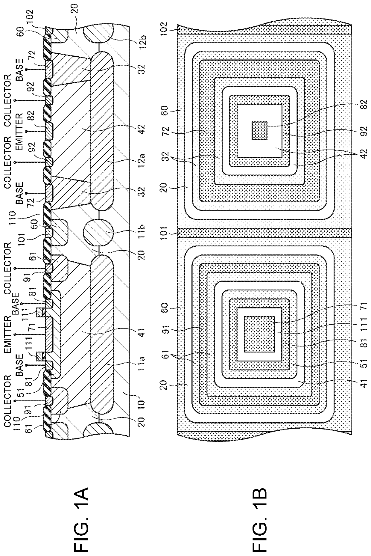
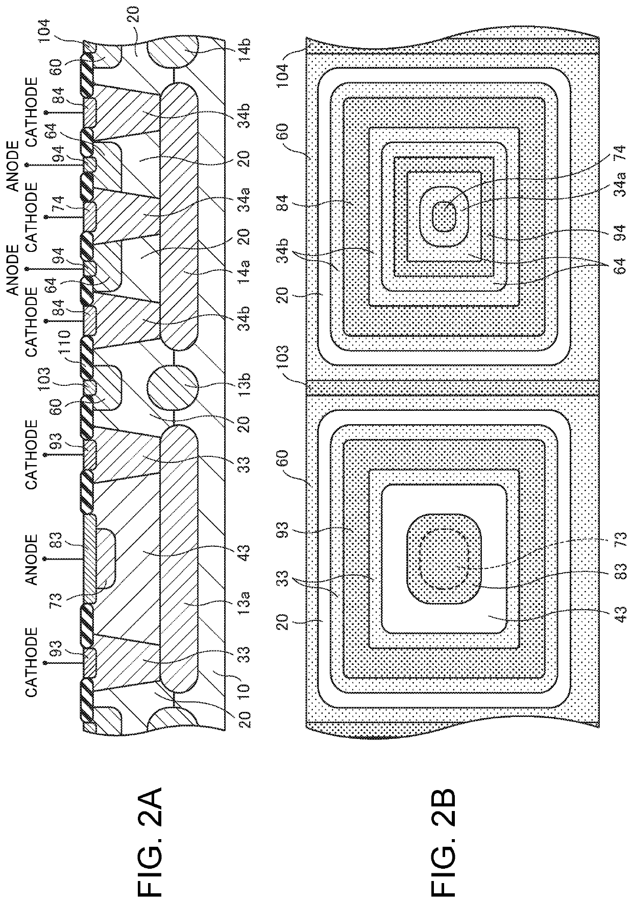
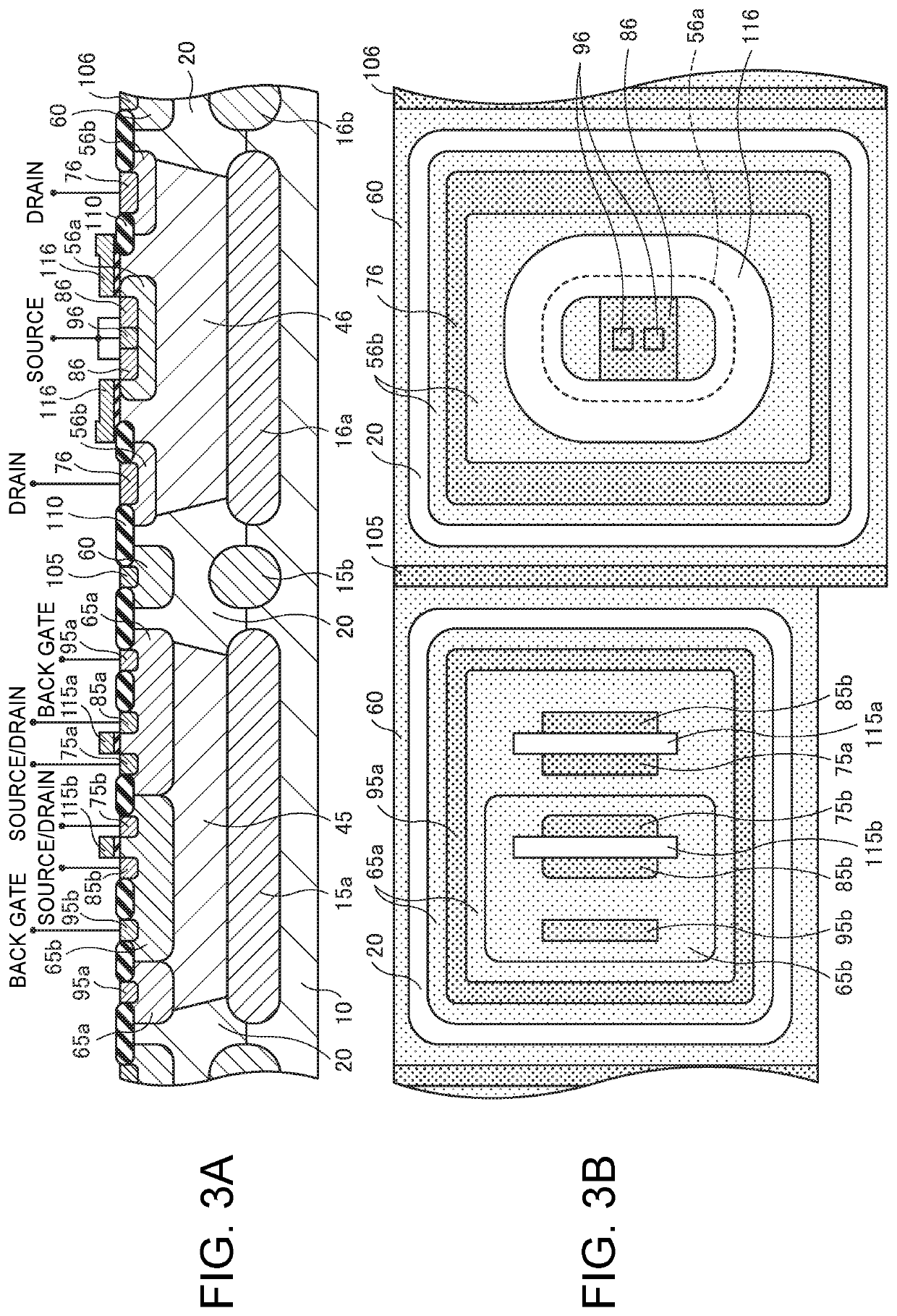
[0032]A semiconductor device according to one embodiment of the invention includes a plurality of different types of circuit elements. Hereinafter, examples of these circuit elements will be described with reference to FIGS. 1A to 4B. Note that the plurality of different types of circuit elements shown in FIGS. 1A to 4B are arranged on the same base substrate 10.

[0033]FIGS. 1A and 1B are diagrams illustrating a first example of the circuit element mounted in the semiconductor device according to one embodiment of the invention. The left side of FIGS. 1A and 1B shows a vertical NPN bipolar transistor, and the right side of FIGS. 1A and 1B shows a lateral PNP bipolar transistor. Also, FIG. 1A is a cross-sectional view and FIG. 1B is a...


PUM

PropertyMeasurementUnit
breakdown voltageaaaaaaaaaa
thicknessaaaaaaaaaa

Abstract

A semiconductor device is provided in which a zener diode having a desired breakdown voltage and a capacitor in which voltage dependence of capacitance is reduced are mounted together, and various circuits are realized. The semiconductor device includes: a semiconductor layer; a first conductivity type well that is arranged in a first region of the semiconductor layer; a first conductivity type first impurity diffusion region that is arranged in the well; a first conductivity type second impurity diffusion region that is arranged in a second region of the semiconductor layer; an insulating film that is arranged on the second impurity diffusion region; an electrode that is arranged on the insulating film; and a second conductivity type third impurity diffusion region that is arranged at least on the first impurity diffusion region.

Description

BACKGROUND[0001]1. Technical Field[0002]The present invention relates to a semiconductor device, a manufacturing method of the semiconductor device, and the like.[0003]2. Related Art[0004]A semiconductor device that includes a capacitor (MOS capacitor) that is formed by using a MOS structure as a circuit element is used, for example. A known MOS capacitor is constituted by a gate electrode formed above a semiconductor substrate via a gate insulating film and a substrate region (hereinafter, also referred to as “electrode region”) that opposes the gate electrode with the gate insulating film being interposed therebetween.[0005]However, in the case where the MOS capacitor is configured by using a substrate region having a low impurity concentration similar to a substrate region in which a MOS field effect transistor is formed, a depletion layer is generated in the electrode region due to inversion of the voltage applied to the gate electrode, and an inversion capacitance is formed. Ac...

Claims


Application Information

Patent Timeline
Patent Type & Authority Patents(United States)
IPC IPC(8): H01L27/082H01L21/8224H01L29/78H01L29/66H01L29/735H01L21/761H01L21/8228H01L29/94H01L29/866H01L27/092H01L29/732H01L21/225H01L27/06H01L27/08H01L29/06H01L29/08H01L29/10H01L29/423
CPCH01L27/0922H01L21/2253H01L29/66181H01L29/7816H01L21/761H01L21/8228H01L29/94H01L21/8224H01L29/732H01L29/66681H01L29/866H01L29/0692H01L29/66106H01L29/0684H01L27/0821H01L29/6625H01L29/735H01L27/0676H01L29/66272H01L27/0814H01L29/1083H01L29/42368H01L29/0878H01L29/0626H01L29/92
Inventor KUWAZAWA, KAZUNOBUSAKUMA, SHIGEYUKINITTA, HIROAKISEKISAWA, MITSUOENDO, TAKEHIRO
Owner SEIKO EPSON CORP
Why Eureka
Try Eureka