
Low noise analog-to-digital converter

a converter and low-noise technology, applied in analogue/digital/analogue conversion, physical parameter compensation/prevention, instruments, etc., can solve the problems of physical occupying significant die area and difficult driving of large-scale sampling capacitors, and achieve the effect of less nois

Active Publication Date: 2020-07-14
ANALOG DEVICES INT UNLTD
View PDF25 Cites 2 Cited by
  • Summary
  • Abstract
  • Description
  • Claims
  • Application Information

AI Technical Summary

Benefits of technology

The patent text describes a technique to reduce noise in an analog-to-digital converter (ADC) circuit. This is achieved by using a dynamic filter circuit that can reduce noise and allow for smaller sampling capacitors which can lead to lower noise conversion and decreased power consumption. Overall, this technique helps to improve the performance of the ADC and make it more efficient.

Problems solved by technology

However, larger sampling capacitors can be difficult to drive and can physically occupy significant die area.

Method used


Image

  • Low noise analog-to-digital converter
  • Low noise analog-to-digital converter
  • Low noise analog-to-digital converter

Examples


Embodiment Construction

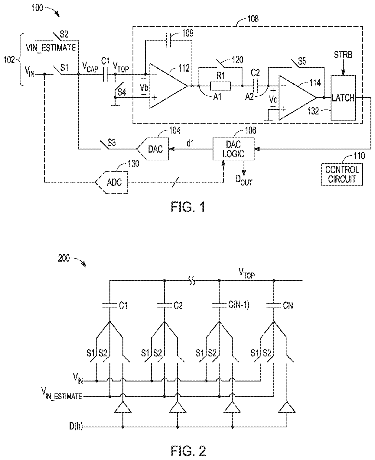
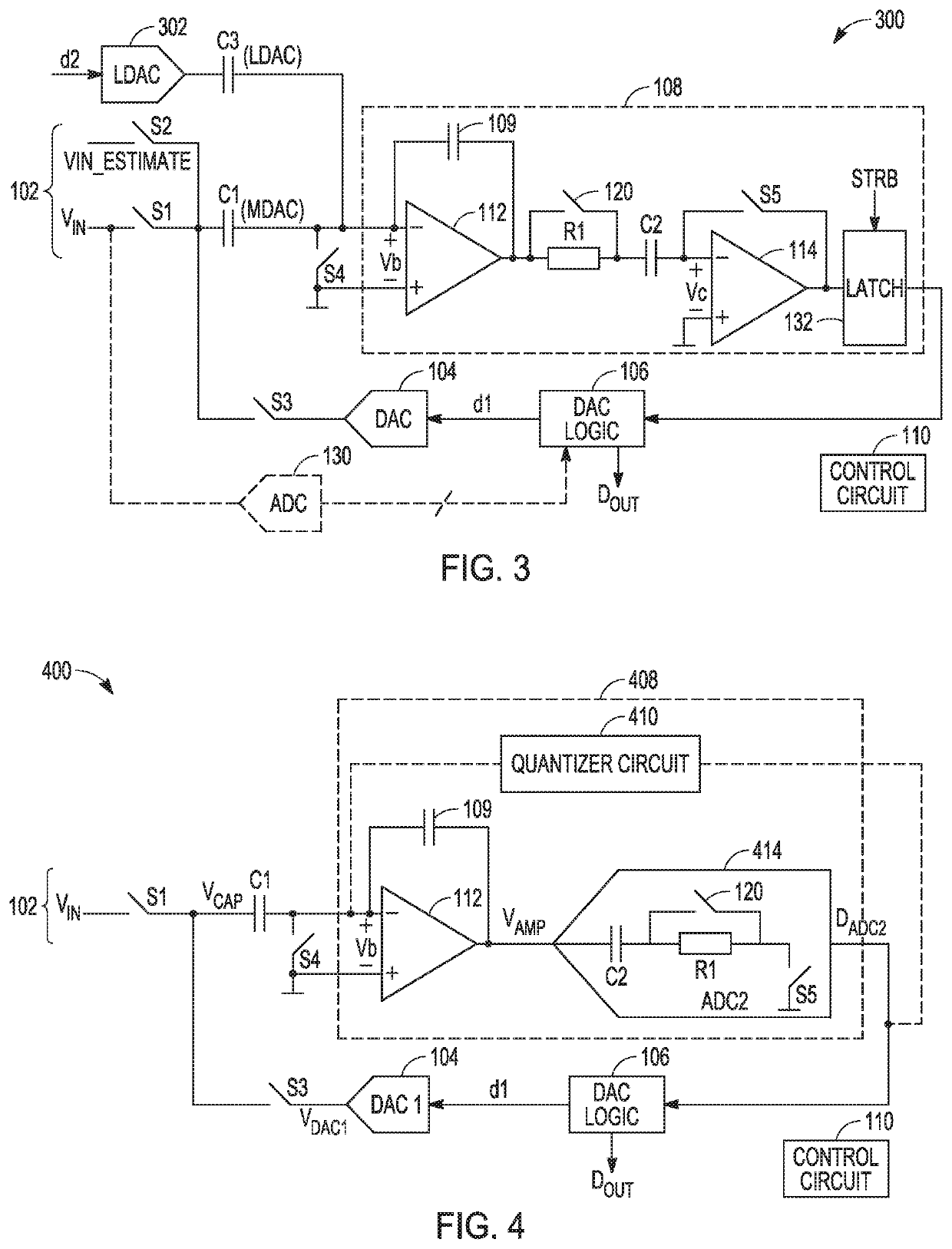
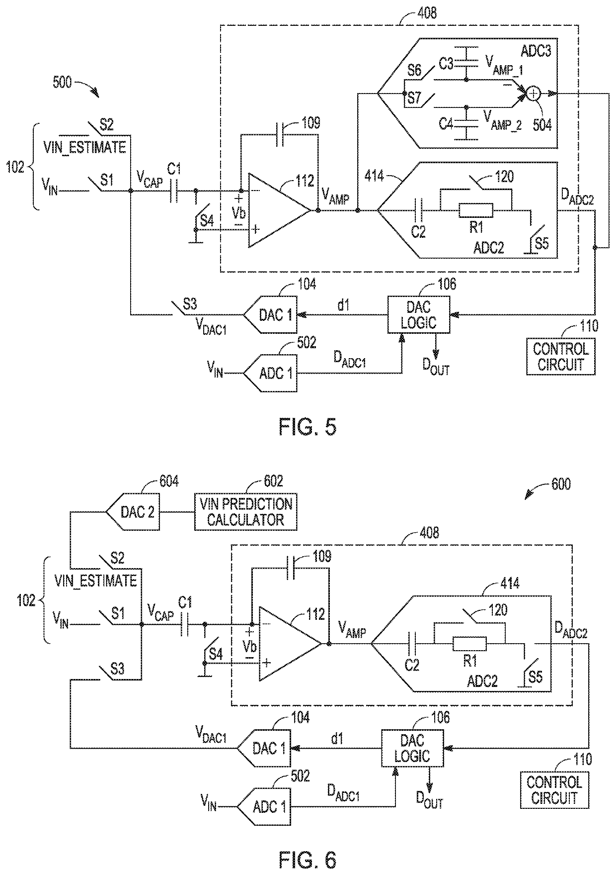
[0036]Various analog-to-digital converter (ADC) topologies exist, including delta-sigma, pipelined converters, flash, and successive approximation register (SAR) converters. Noise sources in an ADC circuit can include kT / C noise of a sampling capacitor, noise coupling on to sampling capacitors from digital circuits and amplifier noise. Also, charge injection from mismatch in sample switches can cause offsets. The kT / C sampling noise is inversely proportional to the size of the sampling capacitors, larger sampling capacitors can produce less noise. However, larger sampling capacitors can be difficult to drive and can physically occupy significant die area.

[0037]By using various techniques of this disclosure, these various noise sources can be largely canceled or reduced. As a result, the size of the sampling capacitors can be greatly reduced, while still achieving significantly improved noise performance and power efficiency for the overall converter. In the following description, va...


PUM


Abstract

Noise sources in an ADC circuit can include kT / C noise of a sampling capacitor, noise coupling on to sampling capacitors from digital circuits, and amplifier noise. Also, charge injection from mismatch in sample switches can cause offsets. These various noise sources can be largely canceled or reduced using described techniques. As a result, the size of the sampling capacitors can be greatly reduced, while still achieving significantly improved noise performance and power efficiency for the overall converter.

Description

FIELD OF THE DISCLOSURE[0001]This document pertains generally, but not by way of limitation, to integrated circuits, and more particularly, to analog to digital converter circuits and systems.BACKGROUND[0002]In many electronics applications, an analog input signal is converted to a digital output signal (e.g., for further digital signal processing). For instance, in precision measurement systems, electronics are provided with one or more sensors to make measurements, and these sensors can generate an analog signal. The analog signal can then be provided to an analog-to-digital converter (ADC) circuit as input to generate a digital output signal for further processing. In another instance, in a mobile device receiver, an antenna can generate an analog signal based on the electromagnetic waves carrying information / signals in the air. The analog signal generated by the antenna can then be provided as input to an ADC to generate a digital output signal for further processing.SUMMARY OF ...

Claims


Application Information

Patent Timeline
Patent Type & Authority Patents(United States)
IPC IPC(8): H03M1/06H03M1/12H03M1/00H03M1/10
CPCH03M1/0626H03M1/06H03M1/1009H03M1/001H03M1/12H03M1/54H03M1/0827H03M1/0863H03M1/08H03M1/1245H03M1/144H03M1/403H03M1/468
Inventor RAJASEKHAR, SANJAYSTEENSGAARD-MADSEN, JESPERLI, HONGXINGHURRELL, CHRISTOPHER PETER
Owner ANALOG DEVICES INT UNLTD
Learn More