Self-gating resistive storage device having resistance transition layer in vertical trench in stacked structure of insulating dielectric layers and electrodes

a dielectric layer and resistance transition technology, applied in the field of microelectronic technology, can solve the problems of low fabrication cost of vertical cross array structure, difficult integration of gating tubes, and saving an expensive lithography step, so as to improve the reliability of the device, the leakage of upper and lower word lines through the gating layer is prevented.

Active Publication Date: 2020-07-21
INST OF MICROELECTRONICS CHINESE ACAD OF SCI
View PDF6 Cites 0 Cited by
  • Summary
  • Abstract
  • Description
  • Claims
  • Application Information

AI Technical Summary

Benefits of technology

[0005]The embodiments of the present invention provide a resistive storage device and a method for fabrication thereof, which are used for solving the technical problem of leakage between upper and lower word lines of a self-gating resistive storage device in the prior art, and improving the reliability of the device.
[0036]One or more of the foregoing technical solutions in the embodiments of the present application at least have the following technical effects:
[0037]The gating layer is grown on the lower electrodes by means of self-alignment technique, such that the interlayer leakage channel running through the gating layer is isolated via the insulating dielectric layers; thus leakage of the upper and lower word lines by means of the gating layer is prevented, solving the technical problem in the prior art of leakage between the upper and lower word lines in a self-gating resistive storage device, and improving the reliability of the device.

Problems solved by technology

Compared with the multilayer stacked structure, the unit in the vertical direction of the three-dimensional array of the vertical structure is formed by filling a trench once, thus greatly saving an expensive lithography step.
Although the fabrication cost of the vertical cross array structure is low, the problem that gating tubes are difficult to integrate is caused because of the absence of a patterning process for a single device, so it is the key of constructing the vertical cross array to develop a resistive device with a self-gating function.
However, since the upper and lower word lines are connected through the gating layer, there is a problem of interlayer leakage.
When the interlayer voltage difference approaches or exceeds the transition voltage of the gating layer 501, high leakage occurs between the upper and lower word lines, resulting in the problem of reliability of the device.

Method used


Image

  • Self-gating resistive storage device having resistance transition layer in vertical trench in stacked structure of insulating dielectric layers and electrodes
  • Self-gating resistive storage device having resistance transition layer in vertical trench in stacked structure of insulating dielectric layers and electrodes
  • Self-gating resistive storage device having resistance transition layer in vertical trench in stacked structure of insulating dielectric layers and electrodes

Examples


Embodiment Construction

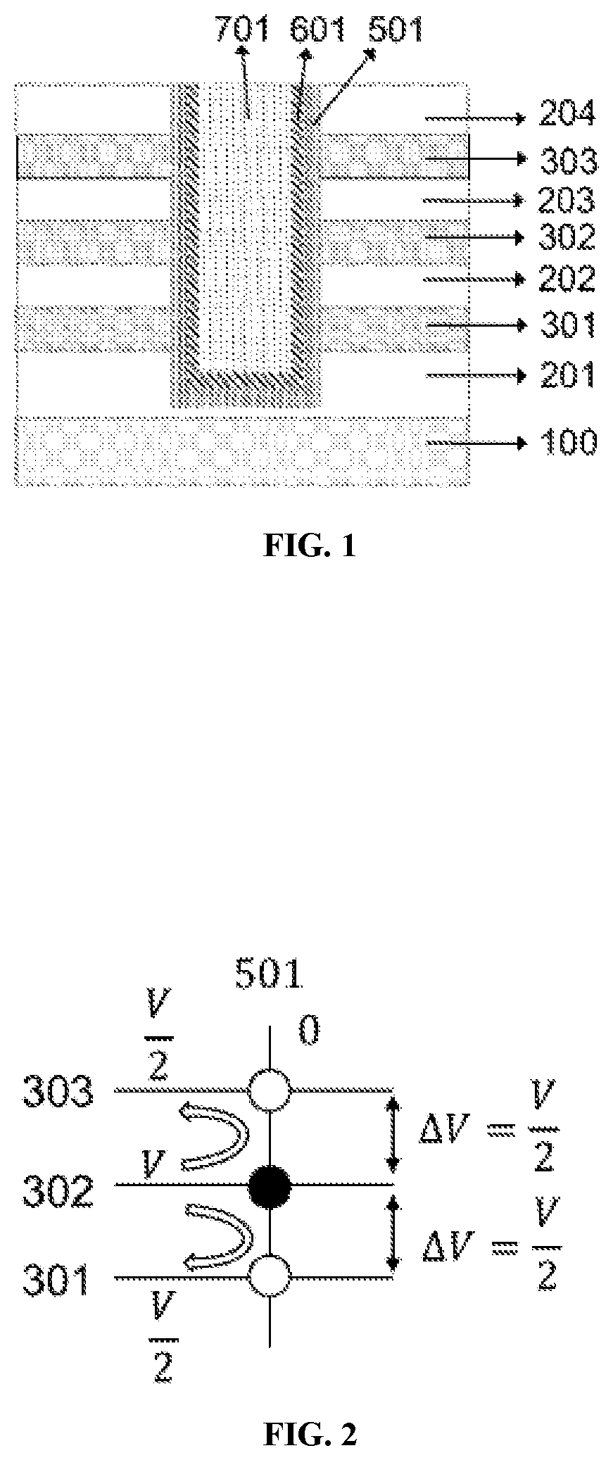
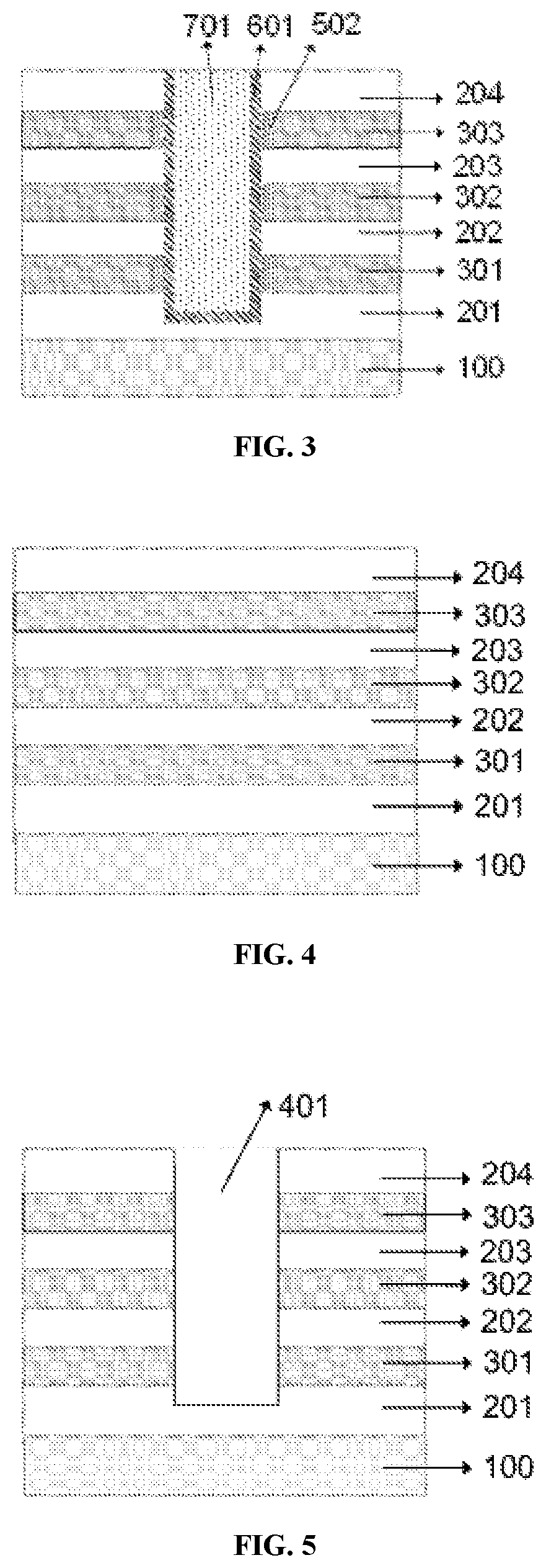
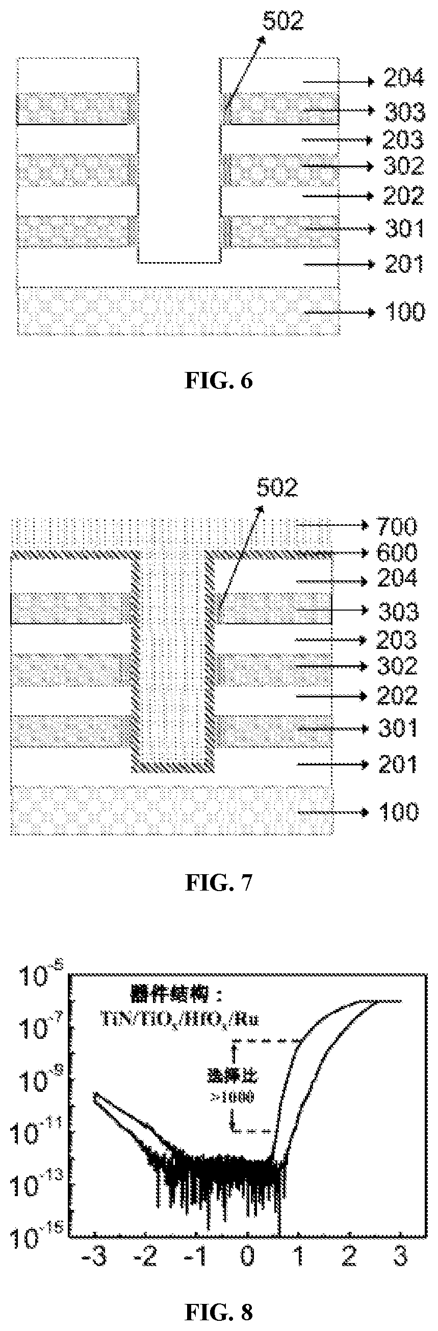
[0047]Exemplary embodiments of the present disclosure will be described in more detail below with reference to the accompanying drawings. Although the drawings show the exemplary embodiments of the present disclosure, it should be understood that the present disclosure may be implemented in various forms and should not be limited to the embodiments illustrated herein. On the contrary, these embodiments are provided so that the present disclosure can be understood more thoroughly, and can fully convey the scope of the present disclosure to those skilled in the art.

[0048]The present invention will be described more fully hereinafter in reference embodiments in combination with the drawings, and the present invention provides preferred embodiments, but should not be regarded as being limited to the embodiments described herein. In the figures, the thicknesses of layers and regions are magnified for clarity, but the schematic diagrams should not be considered to strictly reflect the pro...


PUM

PropertyMeasurementUnit
thicknessesaaaaaaaaaa
thicknessaaaaaaaaaa
thicknessaaaaaaaaaa

Abstract

Provided are a self-gating resistive storage device and a method for fabrication thereof; said self-gating resistive storage device comprises: lower electrodes; insulating dielectric layers arranged perpendicular to, and intersecting with, the lower electrodes to form a stacked structure, said stacked structure being provided with a vertical trench; a gating layer grown on the lower electrodes by means of self-alignment technique, the interlayer leakage channel running through the gating layer being isolated via the insulating dielectric layers; a resistance transition layer arranged in the vertical trench and connected to the insulating dielectric layers and the gating layer; and an upper electrode arranged in the resistance transition layer. In the storage device provided by the described technical solution, the gating layer is grown on the lower electrodes by means of self-alignment technique, such that the interlayer leakage channel running through the gating layer is isolated via the insulating dielectric layers; thus leakage between the upper and lower word lines through the gating layer is prevented, solving the technical problem in the prior art of leakage between the upper and lower word lines in a self-gating resistive storage device, and improving the reliability of the device.

Description

TECHNICAL FIELD[0001]The present invention relates to the field of microelectronic technology, and particularly, relates to a self-gating resistive storage device and method for fabrication thereof.BACKGROUND OF THE INVENTION[0002]A resistive memory is of a metal / oxide / metal (MIM) capacitor structure. Under the action of electrical signals, the device is reversibly converted between a high resistance state (HRS) and a low resistance state (LRS) to realize a data storage function. The resistive memory has attracted great attention at home and abroad due to its excellent characteristics in terms of cell area, three-dimensional integration, low power consumption, high erasing speed, multi-value storage and the like.[0003]There are mainly two three-dimensional integration methods for the resistive memory: one method adopts a cross array multilayer stacked structure, that is, a two-dimensional cross array structure is repeatedly fabricated and stacked in multiple layers; and the other me...

Claims


Application Information

Patent Timeline
Patent Type & Authority Patents(United States)
IPC IPC(8): H01L45/00H01L27/24
CPCH01L45/1608H01L45/14H01L45/142H01L45/1253H01L27/2463H01L45/1675H01L45/1233H01L27/249H01L45/143H01L27/2481H01L45/04H01L45/1226H01L45/146H10B63/845H10N70/823H10N70/20H10N70/8833H10B63/80H10B63/84H10N70/826H10N70/021H10N70/063H10N70/841H10N70/881H10N70/8822H10N70/8825
Inventor LV, HANGBINGLIU, MINGXU, XIAOXINLUO, QINGLIU, QILONG, SHIBING
Owner INST OF MICROELECTRONICS CHINESE ACAD OF SCI
Why Eureka
Try Eureka