Multilayer circuit board structure and manufacturing method thereof

a multi-layer circuit board and manufacturing method technology, applied in the direction of printed circuit aspects, high current circuit adaptations, conductive pattern reinforcement, etc., can solve the problems of reducing the life of the machine and affecting the yield rate, and achieve the effect of product design freedom and preferable yield ra

Active Publication Date: 2020-08-04
UNIMICRON TECH CORP
View PDF9 Cites 0 Cited by
  • Summary
  • Abstract
  • Description
  • Claims
  • Application Information

AI Technical Summary

Benefits of technology

[0005]The invention provides a multilayer circuit board structure that can achieve the hybrid bonding and provide more preferable yield rate and product design freedom.

Problems solved by technology

However, in the above method, the macromolecular dielectric layer is fully coated on the bonding surfaces, and bonding Cu surfaces are exposed by removing unnecessary macromolecular dielectric layer by ways of grinding or cutting.
At the time, since the macromolecular dielectric layer is not completely cured yet, the step of removing the unnecessary macromolecular dielectric layer by ways of grinding or cutting may leads to an adhesion of the macromolecular dielectric layer which not only reduces the life of the machine but also affects the yield rate.

Method used


Image

  • Multilayer circuit board structure and manufacturing method thereof
  • Multilayer circuit board structure and manufacturing method thereof
  • Multilayer circuit board structure and manufacturing method thereof

Examples


Embodiment Construction

[0034]Exemplary embodiments of the invention are described comprehensively with reference to the accompanied drawings. Nonetheless, then invention can still be implemented in a number of different forms, and should not be construed as limited by the embodiments set forth in the disclosure. In the drawings, for clarity, size and thickness of each of regions, parts and layers may not be drawn according to actual proportion. For ease of explanation, the same devices below are provided with the same reference numerals.

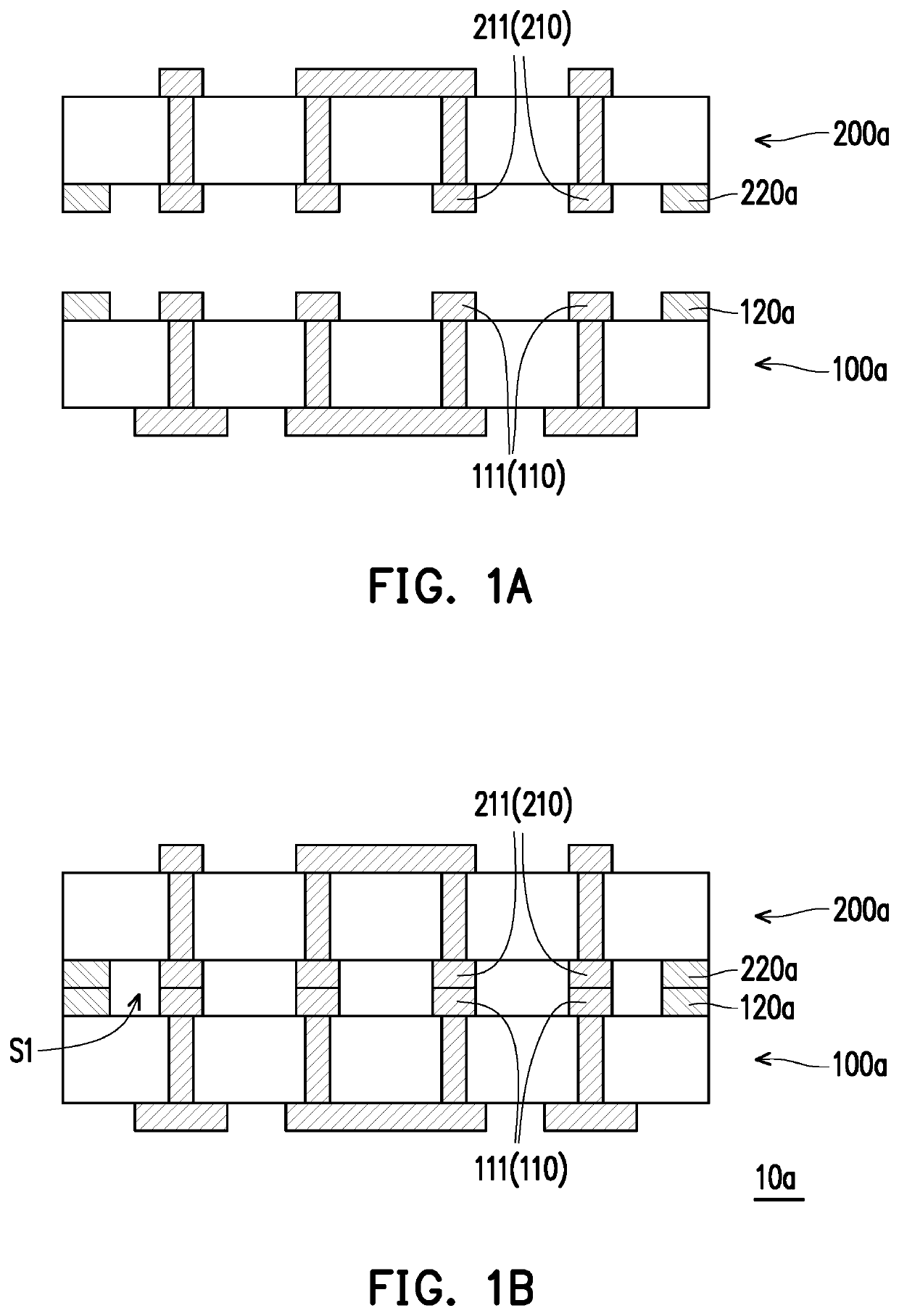
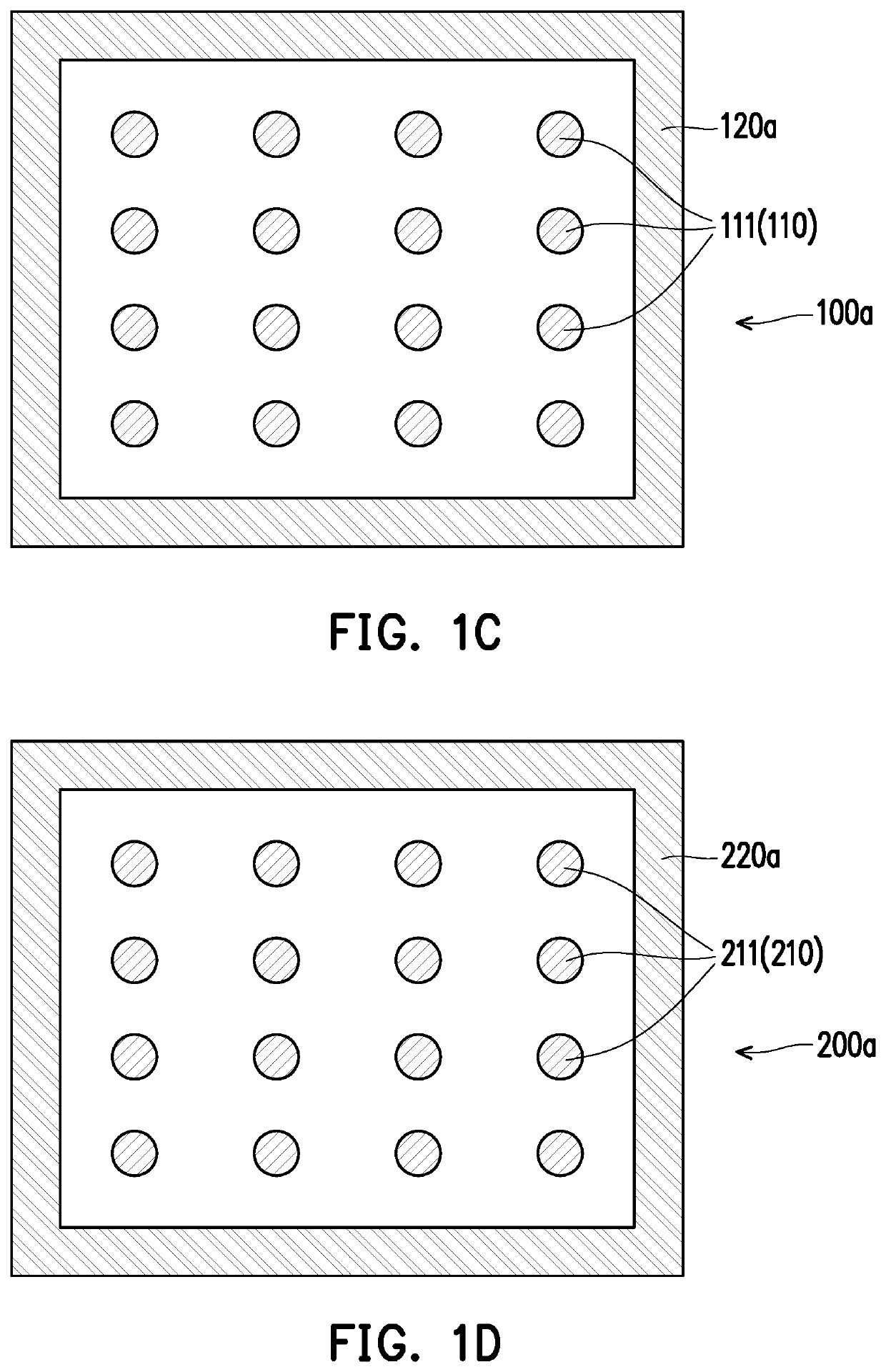
[0035]FIG. 1A and FIG. 1B are cross sectional views for illustrating a manufacturing method of multilayer circuit board structure according to an embodiment of the invention. FIG. 1C is a top view of a first multilayer circuit board of FIG. 1A. FIG. 1D is a bottom view of a second multilayer circuit board of FIG. 1A.

[0036]The manufacturing method of multilayer circuit board structure of the present embodiment includes the following steps. First of all, with reference to FI...


PUM


Abstract

A multilayer circuit board structure includes a first multilayer circuit board and a second multilayer circuit board. The first multilayer circuit board includes a first patterned circuit layer and a first dummy circuit layer. The first dummy circuit layer surrounds the first patterned circuit layer. The second multilayer circuit board is disposed on the first multilayer circuit board, and includes a second patterned circuit layer and a second dummy circuit layer surrounding the second patterned circuit layer. The first patterned circuit layer is bonded to the second patterned circuit layer and the first dummy circuit layer is bonded to the second dummy circuit layer. A hollow space is defined between the first multilayer circuit board and the second multilayer circuit board.

Description

CROSS-REFERENCE TO RELATED APPLICATION[0001]This application claims the priority benefit of Taiwan application serial no. 108114002, filed on Apr. 22, 2019. The entirety of the above-mentioned patent application is hereby incorporated by reference herein and made a part of this specification.BACKGROUND OF THE INVENTION1. Field of the Invention[0002]The invention relates to a circuit board structure and a manufacturing method thereof, and more particularly, to a multilayer circuit board structure and a manufacturing method thereof.2. Description of Related Art[0003]A Cu-to-Cu bonding technology currently used in the circuit boards refers to a process of coating a macromolecular dielectric layer fully on bonding surfaces of two circuit boards before bonding the two circuit boards. Next, a pose cure is performed on the macromolecular dielectric layer so that the macromolecular dielectric layer is fully filled in gaps between Cu-to-Cu bonding surfaces. In this way, a hybrid bonding may ...

Claims


Application Information

Patent Timeline
Patent Type & Authority Patents(United States)
IPC IPC(8): H05K1/02H05K3/46H05K3/32H05K3/24
CPCH05K3/243H05K1/0262H05K1/0263H05K3/328H05K1/0298H05K3/46H05K3/462H05K2201/09781H05K2201/10977H05K2203/085
Inventor LEE, SHAO-CHIENWU, MING-HAOLI, ZONG-HUA
Owner UNIMICRON TECH CORP
Why Eureka
Try Eureka