Semiconductor device and method of manufacturing the same

a semiconductor device and semiconductor technology, applied in the field of semiconductor devices, can solve the problems of affecting the silicide surface of the semiconductor device, deteriorating reliability, and deteriorating the flatness of the semiconductor device b>10/b>, and achieves the effect of reducing the risk of failur

Inactive Publication Date: 2009-07-28
RENESAS ELECTRONICS CORP
View PDF5 Cites 0 Cited by
  • Summary
  • Abstract
  • Description
  • Claims
  • Application Information

AI Technical Summary

Benefits of technology

[0019]According to the above-described method, the surface of the cap metal layer may be flattened. Therefore, the surface of the cap metal layer may be made smooth at the step even when the surface of the cap metal layer has irregularities right after it is formed on the copper layer which is configured to, for example, have a plurality of orientations. Moreover, the layer thickness of the cap metal layer may be made uniform. Thereby, the preferable yield rate, and the excellent uniformity in the resistance of via connection may be maintained when a via is formed on the copper layer. Moreover, the flatness of the semiconductor device may be made preferable. Furthermore, in the present invention the layer thickness of the cap metal layer formed on the copper layer may be made more uniform at the step of removing the copper layer by polishing, because the surface of the copper layer is also flattened.
[0020]Moreover, the barrier metal layer is formed on the insulating film when the cap metal layer is formed, and the barrier metal layer is simultaneously removed when the cap metal layer is flattened. Therefore, a metal material may be prevented from adhering to the surface of the insulating film. Moreover, flattening of the cap metal layer and removing of the barrier metal layer are performed at the same time to obtain the above-described effect without increasing the number of steps. Thereby, the manufacturing cost of the semiconductor device may be suppressed. Furthermore, when, for example, a porous material is used as an insulating film, it becomes easier to form a degenerated layer on the surface of the insulating film, or in the insulating film under a condition that a metal material adheres to the surface of the insulating film when the cap metal layer is formed. However, formation of such a degenerated layer may be suppressed according to the method of manufacturing a semiconductor device of the present invention because the surface of the insulating film is covered with the barrier metal layer when the cap metal layer is formed. Thereby, deterioration in the reliability of leakage, TDDB, and the like may be prevented.
[0021]Here, the step of removing by polishing, and that of flattening by polishing may be performed by the CMP method. Moreover, the cap metal layer may be formed with a material different from that of the barrier metal layer or the copper layer. Under such a configuration, only the copper layer may be removed by proper control of polishing conditions, for example, at the step of removing the copper layer by polishing while the barrier metal layer is left. Moreover, the barrier metal layer may be removed, and, at the same time, the cap metal layer may be prevented from being polished too much when the polishing conditions are properly controlled, for example, at the step of flattening the cap metal layer by polishing.
[0023]According to the semiconductor device with the above-described configuration, the layer thickness of the cap metal layer may be made uniform. Thereby, the preferable yield rate, and the excellent uniformity in the resistance of via connection may be maintained when the via is formed on the copper layer. Furthermore, the preferable flatness of the semiconductor device may be realized.
[0024]According to the present invention, the preferable yield rate, and the excellent uniformity in the resistance of via connection can be maintained in the semiconductor device including the copper interconnect line on the surface of which the cap metal layer is formed.

Problems solved by technology

Moreover, when the insulating interlayer is deposited on the cap metal layer 18 under a state in which the surface of the cap metal layer 18 has irregularities, there is caused a problem that the flatness of the semiconductor device 10 is deteriorated.
There is caused a similar problem to that of the above case even in the semiconductor device disclosed in the Japanese Laid-open patent publication No. 2003-243392, because, when the surface of the cap metal layer has irregularities, the silicide surface of the semiconductor device is affected by the surface irregularity of the cap metal layer.
In addition, when the cap metal layer is formed on the insulating interlayer, the reliability is deteriorated.
Moreover, it is difficult to completely remove the extraneous matter on the surface of the insulating film.

Method used


Image

  • Semiconductor device and method of manufacturing the same
  • Semiconductor device and method of manufacturing the same
  • Semiconductor device and method of manufacturing the same

Examples


example

Example 1

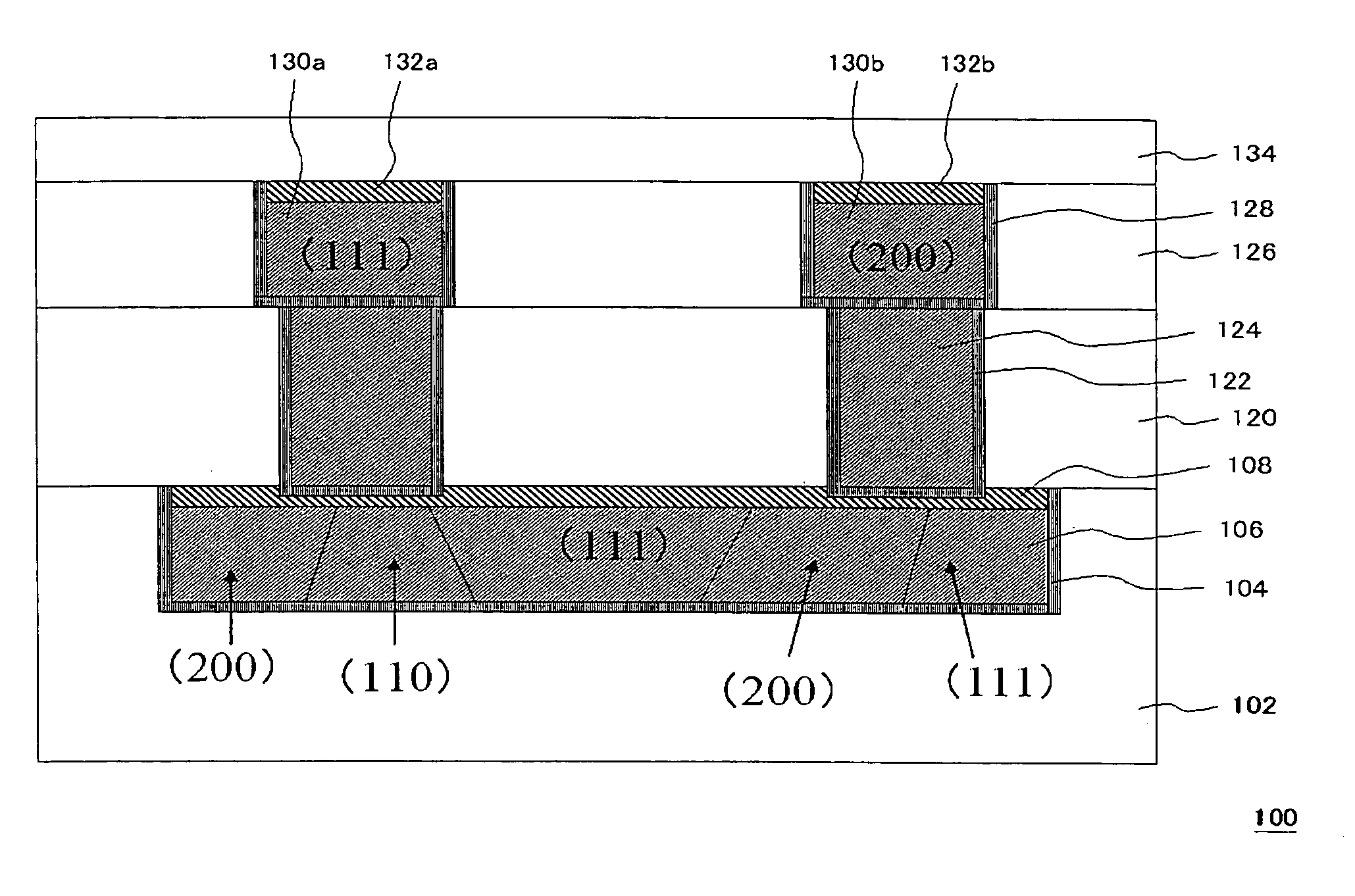
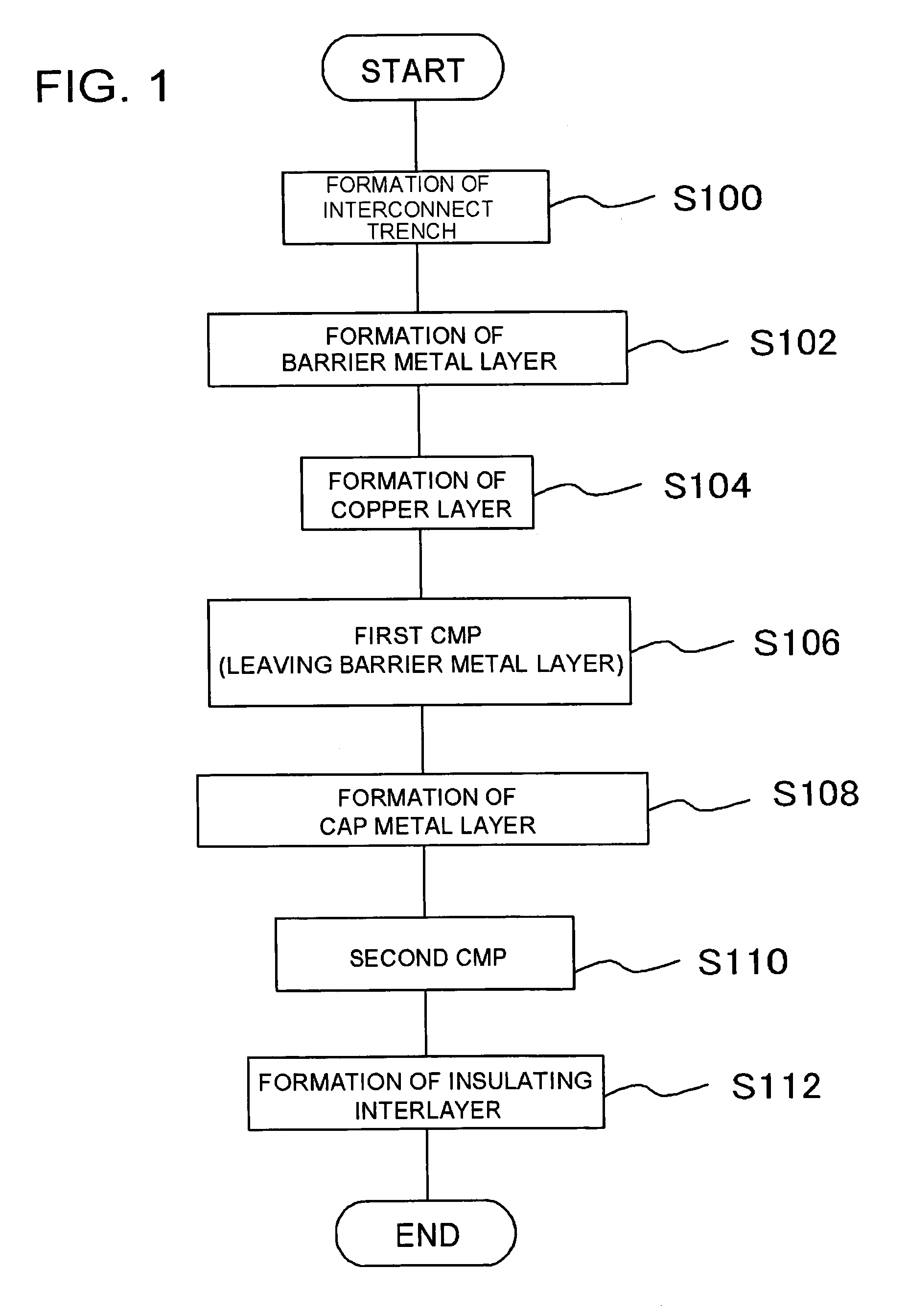
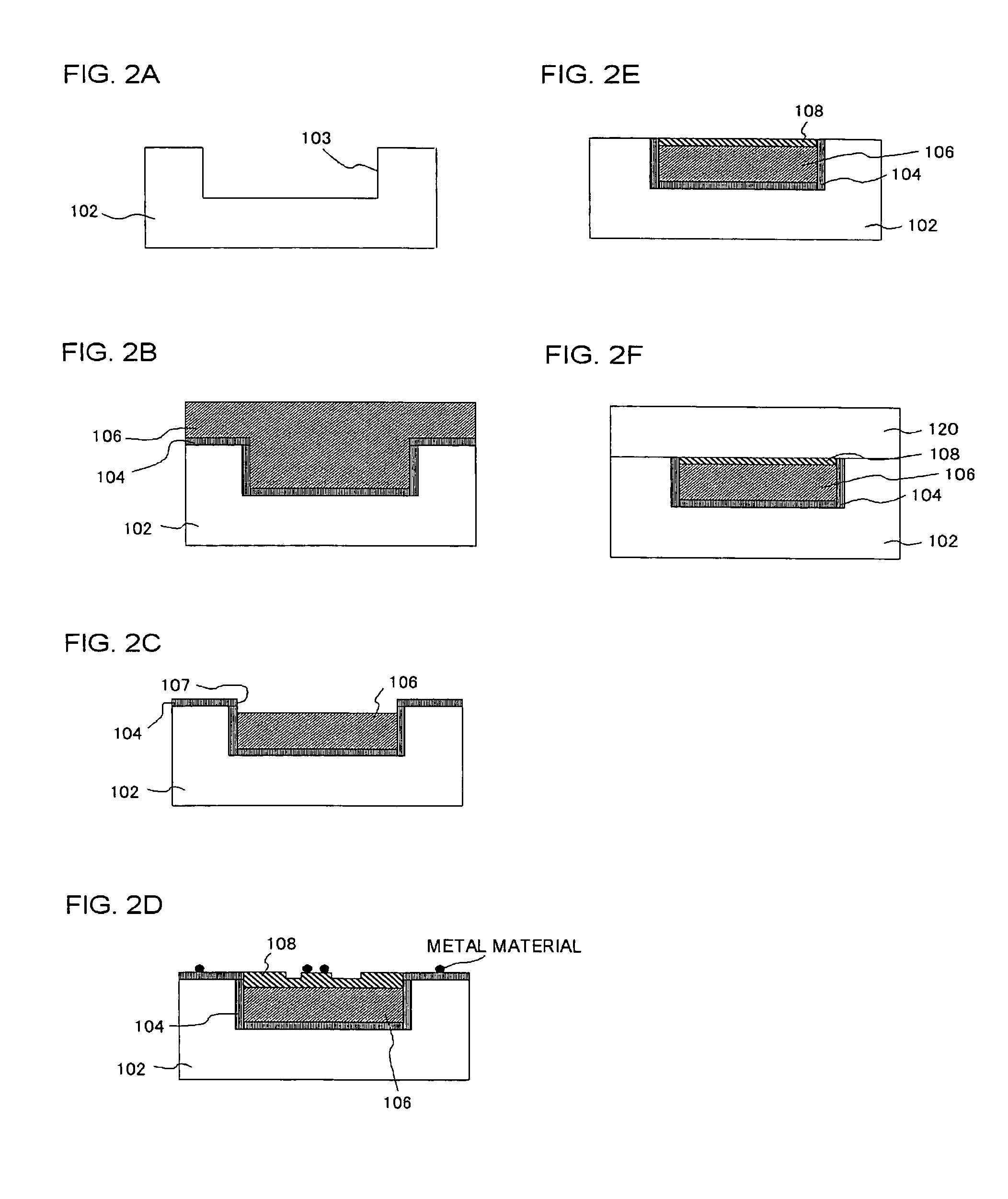
[0066]According to the procedure which has been explained, referring to FIGS. 2A to 2F, the semiconductor device with the configuration shown in FIG. 2F was manufactured. Here, the first insulating interlayer 102 was composed of a SiOC film, the barrier metal layer 104 was composed of a Ta / TaN film, and the cap metal layer 108 was composed of a CoWP film. Firstly, the interconnect trench 103 was formed in the insulating interlayer 102 by dry etching, as shown in FIG. 2A. As shown in FIG. 2B, the TaN film was deposited to a layer thickness of 20 nm, and the Ta film was deposited to a layer thickness of 10 nm to form the barrier metal layer 104. Furthermore, the copper seed layer was deposited to a layer thickness of 100 nm by sputtering, and the copper layer was deposited to a layer thickness to 800 nm by electroplating. Subsequently, the copper layer formed outside the interconnect trench was removed by CMP, as shown in FIG. 2C. At this time, CMP time was adjusted so that a...

example 2

[0067]According to the procedure which has been explained, referring to FIGS. 5A to 5F, the semiconductor device with the configuration shown in FIG. 5E was manufactured. Here, the first insulating interlayer 12 was composed of SiOC film, the barrier metal layer 14 was composed of a Ta / TaN film, and the cap metal layer 18 was composed of a CoWP film. The cap metal layer 18 was formed in a similar manner to that of the cap metal layer 108 in the example 1.

[0068]The surface roughness of the surfaces of the cap metal layers in the semiconductor devices manufactured in the examples 1 and 2 was measured under the following conditions, using an atomic force microscope (AFM).

[0069]Measuring Range: 10 um2;

[0070]Measuring resolution: 0.05 um;

[0071]Step Measuring Range: 20 nm; and

[0072]Step Measuring Accuracy: 0.5 nm

[0073]After the cap metal layer 108 was formed in the example 1, the RMS value of the surface roughness of the cap metal layer 108 was about 2 to 5 nm after the second CMP. Moreov...


PUM

PropertyMeasurementUnit
thicknessaaaaaaaaaa
surface roughnessaaaaaaaaaa

Abstract

The method of manufacturing a semiconductor device according to the present invention includes: forming an interconnect trench in an insulating film formed on a semiconductor substrate (S100); forming a barrier metal layer on the whole surface of the insulating film (S102); forming a copper layer on the whole surface of the barrier metal layer so that the copper layer is embedded in the interconnect trench (S104); removing the copper layer outside the interconnect trench by polishing under a condition that the barrier metal layer is left on the surface of the insulating film (S106); selectively forming a cap metal layer on the copper layer formed in the interconnect trench after the step of removing the copper layer by polishing (S108); and flattening the cap metal layer by polishing (S110).

Description

[0001]This application is based on Japanese Patent application NO. 2005-213593, the content of which is incorporated hereinto by reference.BACKGROUND[0002]1. Technical Field[0003]The present invention relates to a semiconductor device and a method of manufacturing the same.[0004]2. Related Art[0005]Conventionally, there has been known a configuration in which a cap layer having a function as a copper diffusion barrier is formed on copper interconnect lines in a semiconductor device including the copper interconnect lines. There is disclosed a semiconductor device with a configuration in a Japanese Laid-open patent publication No. 2003-243392, wherein a cap layer is formed on metal interconnects including copper, and the cap layer has a silicide surface according to the configuration. According to the Japanese Laid-open patent publication No. 2003-243392, it is possible to effectively prevent oxidation and erosion by hydrofluoric acid by the configuration in which the cap layer has t...

Claims


Application Information

Patent Timeline
Patent Type & Authority Patents(United States)
IPC IPC(8): H01L23/48
CPCH01L21/76849H01L21/7684
Inventor UENO, KAZUYOSHI
Owner RENESAS ELECTRONICS CORP
Why Eureka
Try Eureka