Display device

a technology of display device and display screen, which is applied in the direction of static indicating device, solid-state device, instruments, etc., can solve the problems of light loss, and achieve the effect of preventing from decreasing light transmittan

Active Publication Date: 2020-08-11
LG DISPLAY CO LTD
View PDF9 Cites 0 Cited by
  • Summary
  • Abstract
  • Description
  • Claims
  • Application Information

AI Technical Summary

Benefits of technology

[0006]The present disclosure provides a display device capable of increasing a light transmittance by preventing a loss of light.
[0017]In another aspect of the present disclosure, a display device comprises first to fourth subpixels defined on a substrate and each subpixel having red, white, blue and green emission portions and a non-emission portion; and a first buffer layer disposed on the substrate and including a silicon nitride layer, wherein the silicon nitride layer corresponding to the blue emission portion has a thickness different from those of the silicon nitride layer corresponding to the red, white and green emission portions to prevent from decreasing light transmittance in a range from a green wavelength to a maximum visible light wavelength.
[0018]In a further aspect of the present disclosure, a display device comprises first to fourth subpixels defined on a substrate and each subpixel having red, white, blue and green emission portions and a non-emission portion; and a first buffer layer disposed on the substrate and including a silicon nitride layer and a silicon oxide layer, at least one of the silicon nitride layer and the silicon oxide layer having more than one layers, wherein the at least one of the silicon nitride layer and the silicon oxide layer corresponding to the blue emission portion has a thickness different from those of the silicon nitride layer corresponding to the red, white and green emission portions to prevent from decreasing light transmittance from green and higher wavelength bands.

Problems solved by technology

The silicon nitride layer has a high refractive index of about 1.9 to 2.0, and thus has a problem that a loss of light occurs at an interface between the silicon nitride layer and the silicon oxide layer.

Method used


Image

  • Display device
  • Display device
  • Display device

Examples


Embodiment Construction

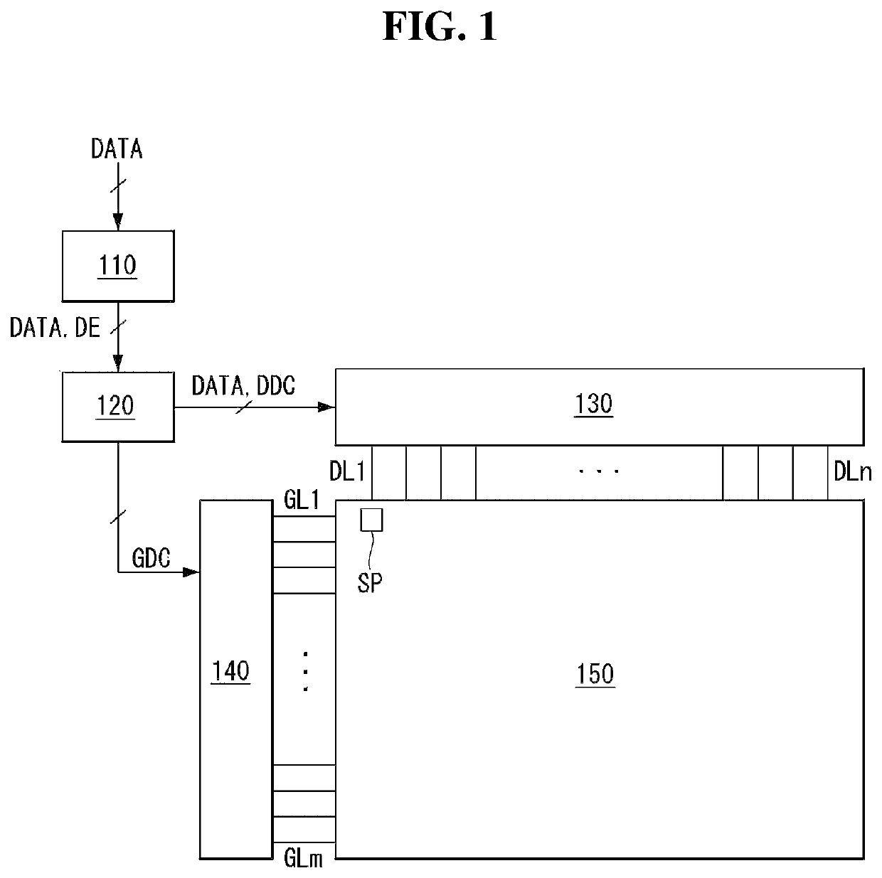
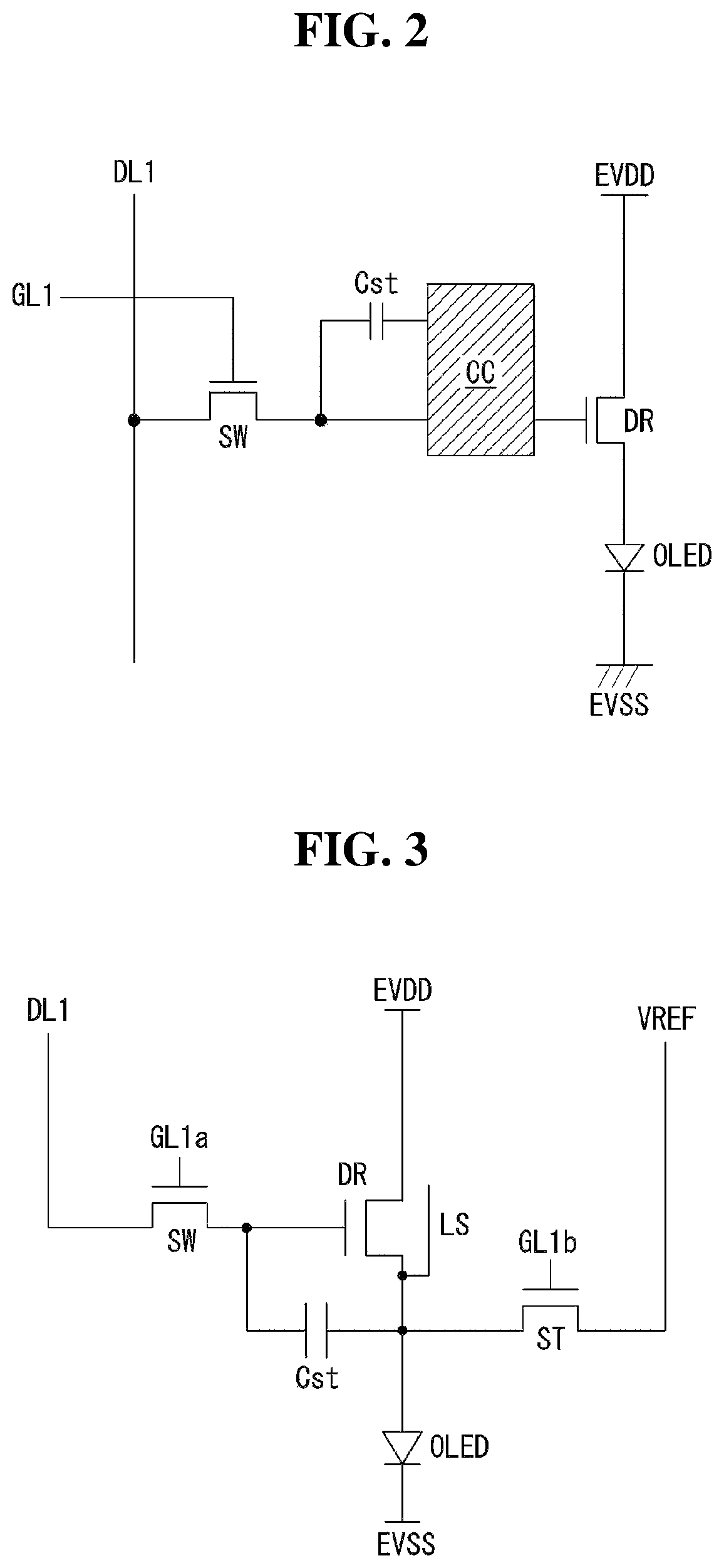
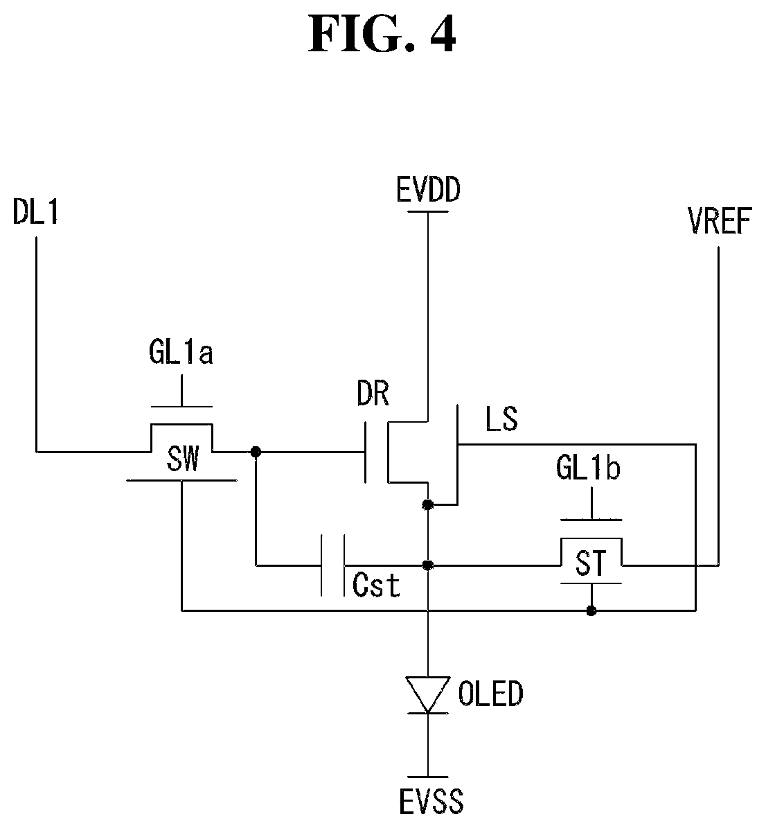
[0031]Reference will now be made in detail to aspects of the disclosure, examples of which are illustrated in the accompanying drawings. Wherever possible, the same reference numbers will be used throughout the drawings to refer to the same or like parts. It will be paid attention that detailed description of known arts will be omitted if it is determined that the arts can mislead aspects of the disclosure. Names of the respective elements used in the following explanations are selected only for convenience of writing the specification and may be thus different from those used in actual products.

[0032]A display device according to an aspect of the disclosure may be implemented as an organic light emitting diode (OLED) display, a liquid crystal display (LCD), an electrophoresis display, and the like. Aspects of the disclosure are described using the OLED display by way of example. An OLED display includes an emission layer that is formed of an organic material between a first electro...


PUM

PropertyMeasurementUnit
refractive indexaaaaaaaaaa
transmittanceaaaaaaaaaa

Abstract

A display device is disclosed. The display device includes a substrate including first to fourth subpixels, a first buffer layer positioned on the substrate, the first buffer layer including a silicon nitride layer and a silicon oxide layer, and a thin film transistor and an organic light emitting diode positioned on the first buffer layer. Each of the first to fourth subpixels includes an emission portion and a non-emission portion. A thickness of the silicon nitride layer in the non-emission portion is greater than a thickness of the silicon nitride layer in the emission portion.

Description

CROSS REFERENCE TO RELATED APPLICATION[0001]This application claims the priority benefit of Korean Patent Application No. 10-2016-0184013 filed on Dec. 30, 2016, which is incorporated herein by reference for all purposes as if fully set forth herein.BACKGROUNDField of the Disclosure[0002]The present disclosure relates to a display device. Although the present disclosure is suitable for a wide scope of application, it is particularly suitable for preventing a loss of light and thereby increasing a light transmittance of the display device.Description of the Background[0003]Various types of flat panel displays (FPDs) have been used to replace heavier and bulkier cathode ray tubes (CRTs). Examples of the flat panel displays include a liquid crystal display (LCD), a field emission display (FED), a plasma display panel (PDP), and an organic light emitting diode (OLED) display. Among them, an OLED display is a self-emission display device emitting light by exciting an organic compound. Th...

Claims


Application Information

Patent Timeline
Patent Type & Authority Patents(United States)
IPC IPC(8): H01L27/32H01L51/00H01L51/52
CPCH01L51/0096H01L51/5262H01L27/3258H01L27/3276H01L27/3213H01L51/5203G09G2310/0264Y02E10/549H10K59/12H10K50/858H10K50/844H10K59/351H10K59/124H10K77/10H10K50/85H01L27/1262H10K59/1213H10K2102/00H10K2102/351H10K50/805H10K59/131
Inventor CHO, MINGUKIM, DOJINKIM, MIAE
Owner LG DISPLAY CO LTD
Why Eureka
Try Eureka