Electronic package
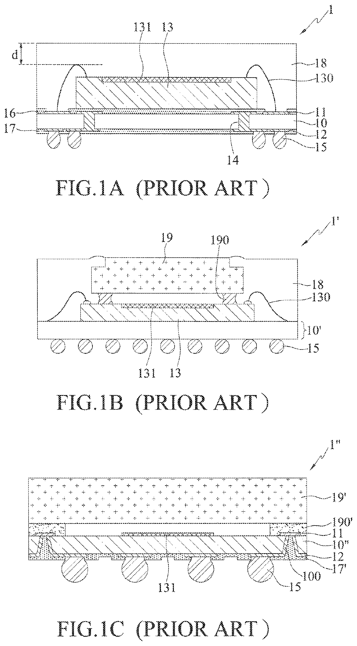
a technology of electronic packaging and encapsulant, which is applied in the direction of electrical apparatus casings/cabinets/drawers, semiconductor/solid-state device details, instruments, etc., can solve the problems of difficult control of the thickness of the encapsulant b>18/b>, inability to achieve the thinning of the wire-bonding type package structure b>1/b>, and difficult to thin the cob type package structure. , to
- Summary
- Abstract
- Description
- Claims
- Application Information
AI Technical Summary
Benefits of technology
Problems solved by technology
Method used
Image
Examples
first embodiment
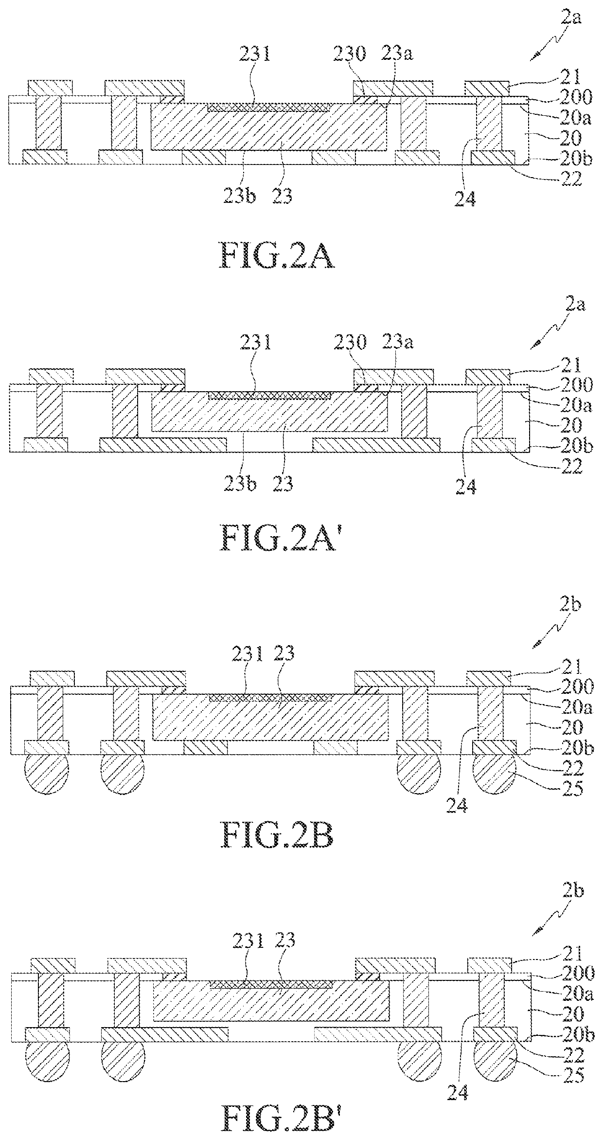
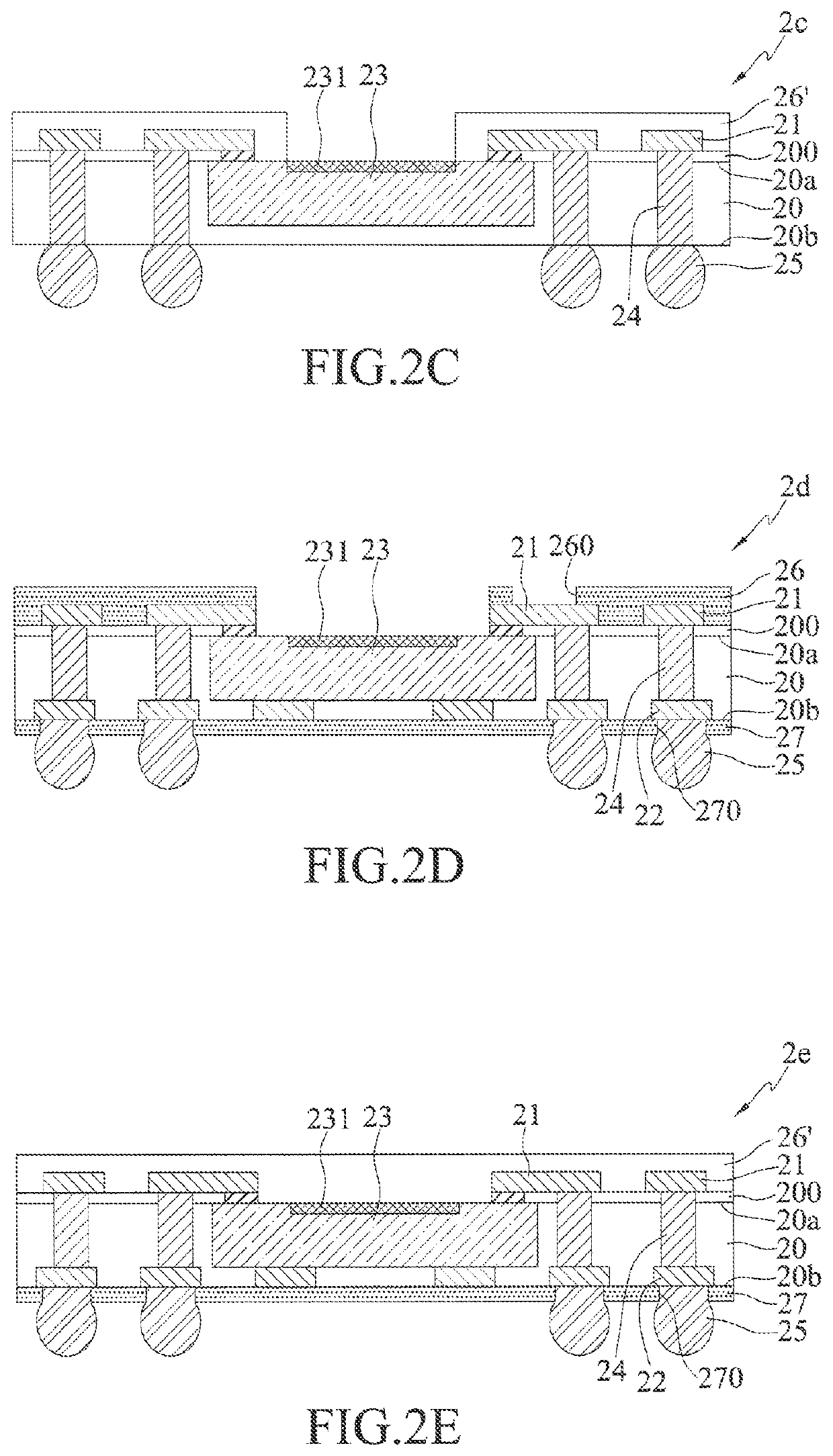
[0042]FIGS. 2A to 2E are schematic cross-sectional views of electronic packages 2a to 2e according to the present disclosure. The electronic packages 2a to 2e are applicable in, for example, fingerprint identifiers and image sensors.
[0043]Referring to FIG. 2A, the electronic package 2a has: a first insulating layer 20 having opposite first and second surfaces 20a, 20b; an electronic element 23 embedded in the first insulating layer 20; a plurality of conductive posts 24 formed in the first insulating layer 20; and a first circuit layer 21 and a second circuit layer 22 formed on the first and second surfaces 20a, 20b of the first insulating layer 20, respectively.
[0044]In the present embodiment, the first insulating layer 20 is made of a molding compound, or a dielectric material such as an epoxy resin, polyimide or other photosensitive or non-photosensitive organic resin. According to the practical need, another insulating layer 200 can be formed on the first surface 20a of the firs...
third embodiment
[0069]FIGS. 4A and 4B are schematic cross-sectional views of electronic packages 4a, 4b according to the present disclosure. The present embodiment differs from the above-described embodiments in that the electronic packages 4a, 4b are applicable in camera lenses. In particular, a transparent element 40 is added.
[0070]Referring to FIGS. 4A and 4B, as compared to FIGS. 2D and 3B, the electronic packages 4a, 4b further has a transparent element 40 such as a lens or glass that covers the sensing area 231 of the electronic element 23. For example, the transparent element 40 is attached to the second insulating layer 26. As such, the present disclosure dispenses with the conventional support members so as to reduce the thickness of the overall structure.
[0071]In the electronic package 4a of FIG. 4A, the surface of the second insulating layer 26 is flush with the surface of the first circuit layer 21.
[0072]On the other hand, in the electronic package 4b of FIG. 4B, the first insulating la...
PUM
| Property | Measurement | Unit |
|---|---|---|
| insulating | aaaaa | aaaaa |
| transparent | aaaaa | aaaaa |
| thickness | aaaaa | aaaaa |
Abstract
Description
Claims
Application Information


