Bias switch circuit for compensating frontend offset of high accuracy measurement circuit

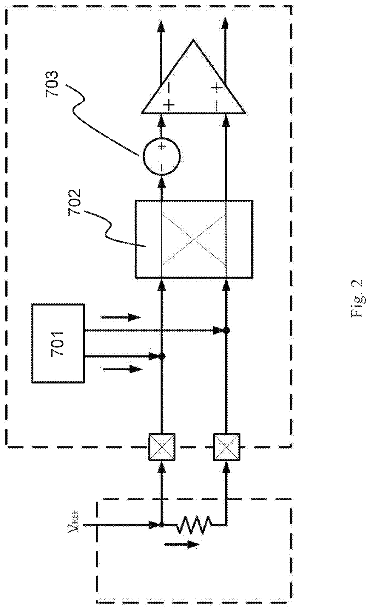
a bias switch and frontend offset technology, applied in the direction of measuring using digital techniques, amplifiers with semiconductor devices/discharge tubes, instruments, etc., can solve the problem of non-ideal effects of measurement circuits, leakage current generated by electrostatic protection circuits b>701/b> in the front end of choppers b>702/b> cannot be compensated, and the offset voltage (vos) of amplifiers can be completely eliminated, improve the compensation

Active Publication Date: 2020-11-03
HYCON TECH
View PDF9 Cites 0 Cited by
  • Summary
  • Abstract
  • Description
  • Claims
  • Application Information

AI Technical Summary

Benefits of technology

[0010]In the above operation method, the higher the input impedance (RS) is, the better the compensation effect is for the leakage current (IL1 and IL2). The reason is during the first timing, when conducting first switch, ideal situation is the leakage current of positive terminal pin (IL1) flowing to the reference voltage instead of the input impedance (RS). The higher input impedance (RS) is, the closer it comes to the ideal situation. During the second timing when conducting second switch, ideal situation is the leakage current of negative terminal pin (IL2) flowing to the reference voltage instead of the input impedance (RS). The higher input impedance (RS) is, the closer it comes to the ideal situation. Thus, the higher the input impedance (RS) is, the better the compensation effect is for the leakage current (IL1 and IL2).
[0011]In the above accurate measurement circuit and the operation method, there is a compensation effect for the leakage current of front end pin but the offset of the amplifier is not eliminated. It is just to adjust the connection of the switches to compensate the leakage current of front end pin and eliminate the offset of the back end amplifier at the same time.
[0013]An operation method of said accurate measurement circuit comprises two timings: a first timing and a second timing. In the first timing, conduct the first switch, the third switch and the sixth switch, turn off the second switch, the fourth switch and the fifth switch. Hence, the positive terminal pin and the positive input of amplifier are connected to the reference voltage, and the negative terminal pin is connected to the negative input of amplifier at the same time. At this moment, voltage of the positive input of amplifier equals to the reference voltage (VREF) added by an offset voltage (VOS) of the amplifier. Mathematical expression is “VREF+VOS”. Voltage of the negative input of amplifier equals to the reference voltage (VREF) subtracted by “current to be measured (IS) subtracted by a leakage current of negative terminal pin (IL2), multiplied by an input impedance (RS)”. Mathematical expression is “VREF−((IS−IL2)*RS)”. Thus, a voltage difference between the positive input of amplifier and the negative input of amplifier is “VOS+(IS−IL2)*RS”. In the second timing, conduct the second switch, the fourth switch and the fifth switch, and turn off the first switch, the third switch and the sixth switch. Hence, the negative terminal pin and the positive input of amplifier are connected to the reference voltage, and the positive terminal pin is connected to the negative input of amplifier at the same time. At this moment, voltage of the positive input of amplifier equals to the reference voltage (VREF) added by the offset voltage (VOS) of the amplifier. Mathematical expression is “VREF+VOS”. Voltage of the negative input of amplifier equals to the reference voltage (VREF) added by “current to be measured (IS) added by a leakage current of positive terminal pin (IL1), and multiplied by an input impedance (RS)”. Mathematical expression is “VREF+((IS+IL1)*RS)”. Thus, a voltage difference between the positive input of amplifier and the negative input of amplifier is “VOS−(IS+IL1)*RS”. Assuming the gain of the amplifier is K, the output voltages generated in the two timings are subtracted and then divided by 2 is “K*(IS+((IL1−IL2) / 2))*RS”. Thus, non-ideal effect of the leakage current of positive terminal pin (IL1) and the leakage current of negative terminal pin (IL2) can be compensated. Meanwhile, the offset voltage (VOS) of the amplifier can be completely eliminated.
[0015]An operation method of said accurate measurement circuit comprises two timings: a first timing and a second timing. The reference voltage of these two timings is fixedly connected to the positive input of amplifier or the negative input of amplifier. In the first timing, conduct the first switch and the fourth switch, and turn off the second switch and the third switch. Hence, the positive terminal pin is connected to the positive input of amplifier, and the negative terminal pin is connected to the negative input of amplifier at the same time. Evaluate a condition according to that the reference voltage is connected to the positive input of amplifier, a voltage difference between the positive input of amplifier and the negative input of amplifier is “VOS−(IS−IL2)*RS”. In the second timing, conduct the second switch and the third switch, and turn off the first switch and the fourth switch. Hence, the positive terminal pin is connected to the negative input of amplifier, and the negative terminal pin is connected to the positive input of amplifier at the same time. Evaluate a condition according to that the reference voltage is connected to the positive input of amplifier, a voltage difference between the positive input of amplifier and the negative input of amplifier is “VOS−(IS+IL1)*RS”. Assuming the gain of the amplifier is K, the output voltages generated in the two timings are subtracted and then divided by 2 is “K*(IS+(IL1−IL2) / 2))*RS”. Thus, non-ideal effect of the leakage current of positive terminal pin (IL1) and the leakage current of negative terminal pin (IL2) can be compensated. Meanwhile, the offset voltage (VOS) of the amplifier can be completely eliminated.
[0018]An operation method of said accurate measurement circuit comprises two timings: a first timing and a second timing. In the first timing, conduct the first switch and the fourth switch, and turn off the second switch and the third switch. Hence, the positive terminal pin is connected to the positive input of amplifier, and the negative terminal pin is connected to the reference voltage. Thus, the voltage of the positive input of amplifier is “VREF+VOS+(IS+IL1)*RS”. In the second timing, conduct the second switch and the third switch, and turn off the first switch and the fourth switch. Hence, the positive terminal pin is connected to the reference voltage, and the negative terminal pin is connected to the positive input of amplifier. Thus, the voltage of the positive input of amplifier is “VREF+VOS−(IS−IL2)*RS”. Assuming the gain of the amplifier is K, the output voltages generated in the two timings are subtracted and then divided by 2 is “K*(IS+((IL1−IL2) / 2))*RS”. Thus, non-ideal effect of the leakage current of positive terminal pin (IL1) and the leakage current of negative terminal pin (IL2) can be compensated. Meanwhile, the offset voltage (VOS) of the amplifier can be completely eliminated.
[0020]In the operation method mentioned above, the higher the input impedance (RS) is, the better the compensation effect is for the leakage current (IL1 and IL2). The reason is during the first timing, when conducting first switch, ideal situation is the leakage current of positive terminal pin (IL1) flowing to the reference voltage instead of the input impedance (RS). The higher input impedance (RS) is, the closer it comes to the ideal situation. During the second timing when conducting second switch, ideal situation is the leakage current of negative terminal pin (IL2) flowing to the reference voltage instead of the input impedance (RS). The higher input impedance (RS) is, the closer it comes to the ideal situation. Thus, the higher the input impedance (RS) is, the better the compensation effect is for the leakage current (IL1 and IL2).

Problems solved by technology

However, there are some non-ideal effects in the measurement circuit.
For example, leakage current of the components and offsets of low noise amplifiers and analog-to-digital converters all affect the accuracy of measurements.
However, leakage current generated by an electrostatic protection circuit 701 in the front end of the chopper 702 cannot be compensated.
But in the actual measurement environment, there are non-ideal effects in the circuit between the measurement terminal and inside of the chip.
For example, if there are leakage currents in the package pins of a chip or differential circuits at both ends do not match, it will also cause an offset.

Method used


Image

  • Bias switch circuit for compensating frontend offset of high accuracy measurement circuit
  • Bias switch circuit for compensating frontend offset of high accuracy measurement circuit
  • Bias switch circuit for compensating frontend offset of high accuracy measurement circuit

Examples


first embodiment

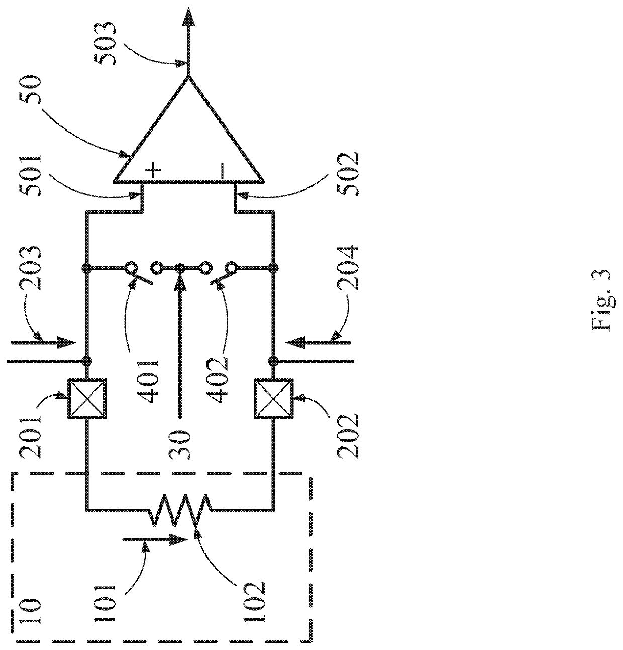
[0034]the present invention is disclosed in FIG. 3. It shows an accurate measurement circuit utilizing a switching circuit for compensating the offset in the front end. The accurate measurement circuit comprises an amplifier 50 and two switches. One terminal of a first switch 401 is connected to a positive input of amplifier 501, and the other terminal is connected to a reference voltage 30. One terminal of a second switch 402 is connected to a negative input of amplifier 502, and the other terminal is connected to the reference voltage 30. The positive input of amplifier 501 and the negative input of amplifier 502 are connected to a measurement terminal 10 via a positive terminal pin 201 and a negative terminal pin 202, respectively.

[0035]An operation method of above accurate measurement circuit comprises two timings: a first timing and a second timing. In the first timing, conduct the first switch 401, and turn off the second switch 402. Hence, the positive input of amplifier 501 ...

second embodiment

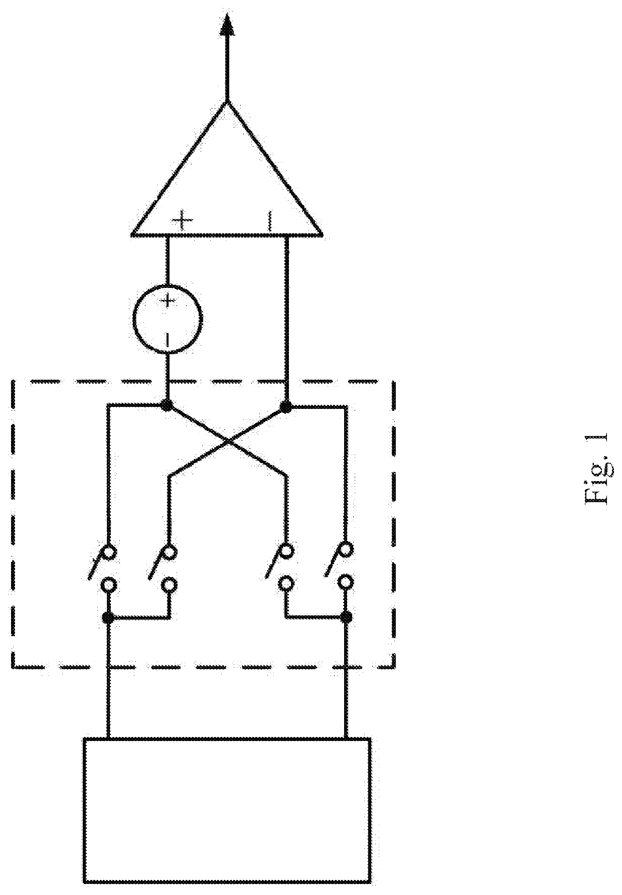
[0040]the present invention is disclosed in FIG. 5. It shows a switching circuit architecture compensating the offset in the front end and eliminating the offset of the amplifier. The accurate measurement circuit comprises an amplifier 50 and six switches. A first switch 401 is connected between a reference voltage 30 and a positive terminal pin 201. A second switch 402 is connected between the reference voltage 30 and a negative terminal pin 202. A third switch 403 is connected between the positive terminal pin 201 and a positive input of amplifier 501. A fourth switch 404 is connected between the positive terminal pin 201 and a negative input of amplifier 502. A fifth switch 405 is connected between the negative terminal pin 202 and the positive input of amplifier 501. A sixth switch 406 is connected between the negative terminal pin 202 and the negative input of amplifier 502.

[0041]An operation method of above accurate measurement circuit comprises two timings: a first timing and...

third embodiment

[0044]the present invention is disclosed in FIG. 7. It shows another switching circuit architecture compensating the offset in the front end and eliminating the offset of the amplifier. The accurate measurement circuit comprises an amplifier 50 and 4 switches. A first switch 401 is connected between a positive terminal pin 201 and a positive input of amplifier 501. A second switch 402 is connected between the positive terminal pin 201 and a negative input of amplifier 502. A third switch 403 is connected between a negative terminal pin 202 and the positive input of amplifier 501. A fourth switch 404 is connected between the negative terminal pin 202 and the negative input of amplifier 502. A reference voltage 30 is directly connected to the positive input of amplifier 501 (as shown in FIG. 7A) or the negative input of amplifier 502 (as shown in FIG. 7B). The positive terminal pin 201 and the negative terminal pin 202 are used to connect to a measurement terminal 10.

[0045]An operatio...


PUM


Abstract

Disclosed is a high accurate measurement circuit, and the feature is using bias switching circuit for compensating front end offset, and the back end offset of amplifier is also cancelled. In the real measurement environment, offset exists in the amplifier of the measurement circuit has, and non-ideal effects also exist in the interface between measurement terminal and the measurement circuit, such as leakage current of chip package pins or mismatch of the circuit. The above non-ideal effects belong to front end offset and cannot be compensated by the prior arts. The disclosed structure uses the bias switch circuit and uses different switching method in the two measurement timings. By subtracting the measurement results for the two measurement timings, the front end offset is compensated, and the back end offset of the amplifier is also cancelled.

Description

FIELD OF THE INVENTION[0001]The present invention relates to a high accurate measurement circuit. More particularly, the present invention relates to a measurement circuit utilizing a bias switching circuit to compensate offset of the front end circuit, further increasing accuracy of measurement.BACKGROUND OF THE INVENTION[0002]Circuits to measure voltage or current are widely used in various electronic components. They usually use low noise amplifiers and analog-to-digital converters to convert voltage or current into digital output. However, there are some non-ideal effects in the measurement circuit. For example, leakage current of the components and offsets of low noise amplifiers and analog-to-digital converters all affect the accuracy of measurements.[0003]Taiwan patent no. 1543544 discloses an architecture comprising a plurality of capacitor pairs and a plurality of switches, and an operation method utilizing switches to transfer electric charges to eliminate gain errors of t...

Claims


Application Information

Patent Timeline
Patent Type & Authority Patents(United States)
IPC IPC(8): H03F3/45H03F1/30H03F3/393G01R19/00
CPCH03F3/393H03F3/45179G01R19/0053H03F3/45753H03F1/301G01R19/25H03F3/45475H03F2203/45614H03F3/387H03F3/45614H03F3/45627H03F3/45623H03F2200/261G01R1/30
Inventor CHAO, PO-YINCHEN, HUNG-WEILEE, SHUI-CHU
Owner HYCON TECH
Why Eureka
Try Eureka