Formation of crystalline, layered transition metal dichalcogenides

a technology of transition metal dichalcogenide and layered metal, which is applied in the direction of selenium/tellurium compunds, coatings, chemistry apparatus and processes, etc., can solve the problems of increasing the size of the substrate used and the difficulty of scaling the cvd process to form layered transition metal dichalcogenides on substrates of increasing diameters

Active Publication Date: 2021-02-09
APPLIED MATERIALS INC
View PDF12 Cites 0 Cited by
  • Summary
  • Abstract
  • Description
  • Claims
  • Application Information

AI Technical Summary

Problems solved by technology

As electronics applications develop, the size of the substrates used increases, and current processes are not configured to scale up to larger substrates for commercial production.
For example, currently, chemical vapor deposition (CVD) is typically used to form the layered transition metal dichalcogenides, but it is challenging to scale the CVD process to form the layered transition metal dichalcogenides on substrates of increasing diameters.

Method used


Image

  • Formation of crystalline, layered transition metal dichalcogenides
  • Formation of crystalline, layered transition metal dichalcogenides
  • Formation of crystalline, layered transition metal dichalcogenides

Examples


Embodiment Construction

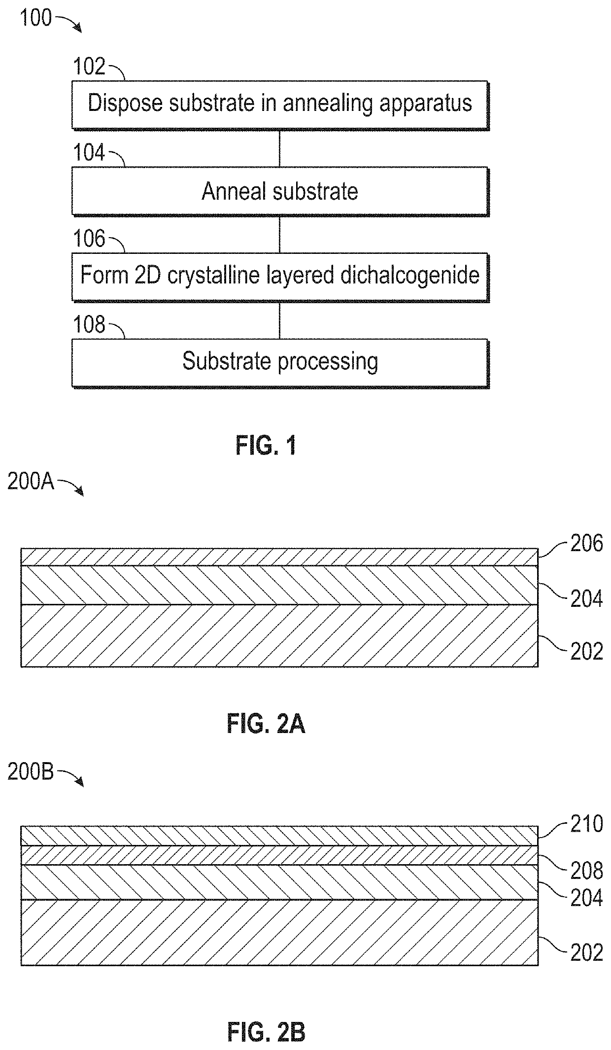
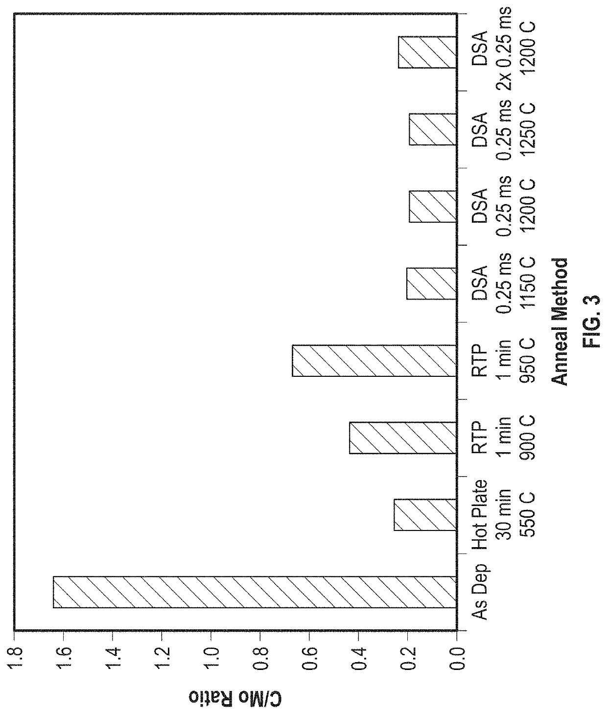
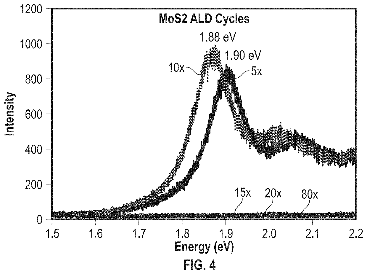
[0017]Two-dimensional crystalline structures are formed on substrates as discussed herein. In particular, two-dimensional crystalline transition metal dichalcogenides are formed herein using an amorphous film formed, in some examples, by atomic layer deposition (ALD) or other methods that deposit uniform films on substrates that can be from, for example, 150 nm to 450 nm in diameter. Conventional chemical vapor deposition (CVD) is traditionally used to form layered transition metal dichalcogenides. However, as substrate diameters increase along with industry demand for high volumes of electronics that use substrates with the increasing diameters, some CVD processes may not have the ability to form a uniform layered transition metal dichalcogenide film. Challenges with conventional CVD processes include precursor volatility and temperature dependency of the deposition. Thus, as substrates increase in diameter, it becomes difficult to maintain temperature uniformity across a substrate...


PUM

PropertyMeasurementUnit
temperatureaaaaaaaaaa
thicknessaaaaaaaaaa
temperatureaaaaaaaaaa

Abstract

Embodiments of the present disclosure relate to forming a two-dimensional crystalline dichalcogenide by positioning a substrate in an annealing apparatus. The substrate includes an amorphous film of a transition metal and a chalcogenide. The film is annealed at a temperature from 500° C. to 1200° C. In response to the annealing, a two-dimensional crystalline structure is formed from the film. The two-dimensional crystalline structure is according to a formula MX2, M includes one or more of molybdenum (Mo) or tungsten (W) and X includes one or more of sulfur (S), selenium (Se), or tellurium (Te).

Description

CROSS-REFERENCE TO RELATED APPLICATIONS[0001]This application claims priority to U.S. Provisional Patent Application Ser. No. 62 / 676,317, filed on May 25, 2018, which herein is incorporated by reference.BACKGROUNDField[0002]Embodiments of the present invention generally relate to the fabrication of substrates used in semiconductors.Description of the Related Art[0003]Layered transition metal dichalcogenides are two-dimensional semiconducting materials used in electronics. Transition metal dichalcogenides exhibit properties such as a direct band gap, strong spin-orbit coupling, and a lack of an inversion center, that makes transition metal dichalcogenides desirable for electronics applications. As electronics applications develop, the size of the substrates used increases, and current processes are not configured to scale up to larger substrates for commercial production. For example, currently, chemical vapor deposition (CVD) is typically used to form the layered transition metal di...

Claims


Application Information

Patent Timeline
Patent Type & Authority Patents(United States)
IPC IPC(8): H01L21/02C23C16/30C23C16/455C23C16/02H01L21/67C01B19/00
CPCH01L21/02686C01B19/007C23C16/0209C23C16/305C23C16/45527H01L21/02499H01L21/02568H01L21/67098C01P2002/01C01P2002/20C23C16/56H01L21/02485H01L21/02488H01L21/02614
Inventor WONG, KEITH TATSEUNNEMANI, SRINIVAS D.YIEH, ELLIE Y.
Owner APPLIED MATERIALS INC
Why Eureka
Try Eureka