Pattern formation method, pattern, and device

A pattern, silane compound technology, applied in electrical components, chemical instruments and methods, photoengraving process of pattern surface, etc., can solve the problems of expensive model, large waste, and difficult to obtain dense silicon oxide film.

Inactive Publication Date: 2012-03-21
JAPAN SCI & TECH CORP
View PDF9 Cites 0 Cited by
  • Summary
  • Abstract
  • Description
  • Claims
  • Application Information

AI Technical Summary

Problems solved by technology

However, in this method, since a gas-phase process is used, there are problems in that large-scale equipment is required, raw material usage efficiency is low, handling is difficult because the raw material is gas, and a large amount of waste is generated.
However, although the process cost of the nanoimprint process itself is low, there is a problem that the model of the pattern (element type) is expensive
Moreover, the more essential problem of this technique is that the resin materials that can be patterned are limited to organic resin materials such as thermoplastic resins, thermosetting resins, and photocurable resins, so they cannot be applied to silicon films or silicon oxide films of the above-mentioned semiconductor elements at all.
Since the outcome of this technology is the sol-gel method, it inherits the disadvantages of the above-mentioned sol-gel method, such as difficulty in obtaining a dense silicon oxide film, easy occurrence of cracks in the film, and inapplicability to plastic substrates with low heat resistance. In addition, it is impossible to form a patterned silicon film in principle

Method used


Image

  • Pattern formation method, pattern, and device
  • Pattern formation method, pattern, and device
  • Pattern formation method, pattern, and device

Examples


Embodiment

[0104] Unless otherwise specified, the following operations were performed in nitrogen with an oxygen concentration of 1 ppm or less.

[0105] The weight average molecular weights of the higher silane compounds in the following synthesis examples and the silicone resins in the comparative examples are obtained from the data of gel permeation chromatography (GPC) measured under the following conditions using the following measuring device, respectively. Styrene converted value.

[0106] The viscosity of the high-grade silane composition is a value measured using the measuring device described below.

[0107]

[0108] Measuring device: manufactured by Agilent Technologies, model "1200 series"

[0109] Column: "Packed column for HPLC KF-G" and "Packed column for HPLC K-805L" manufactured by Showa Denko Co., Ltd. were used in series.

[0110] Solvent: In the determination of advanced silane compounds, cyclohexene is used as the solvent; in the determination of silicone resin, ...

manufacture example 1

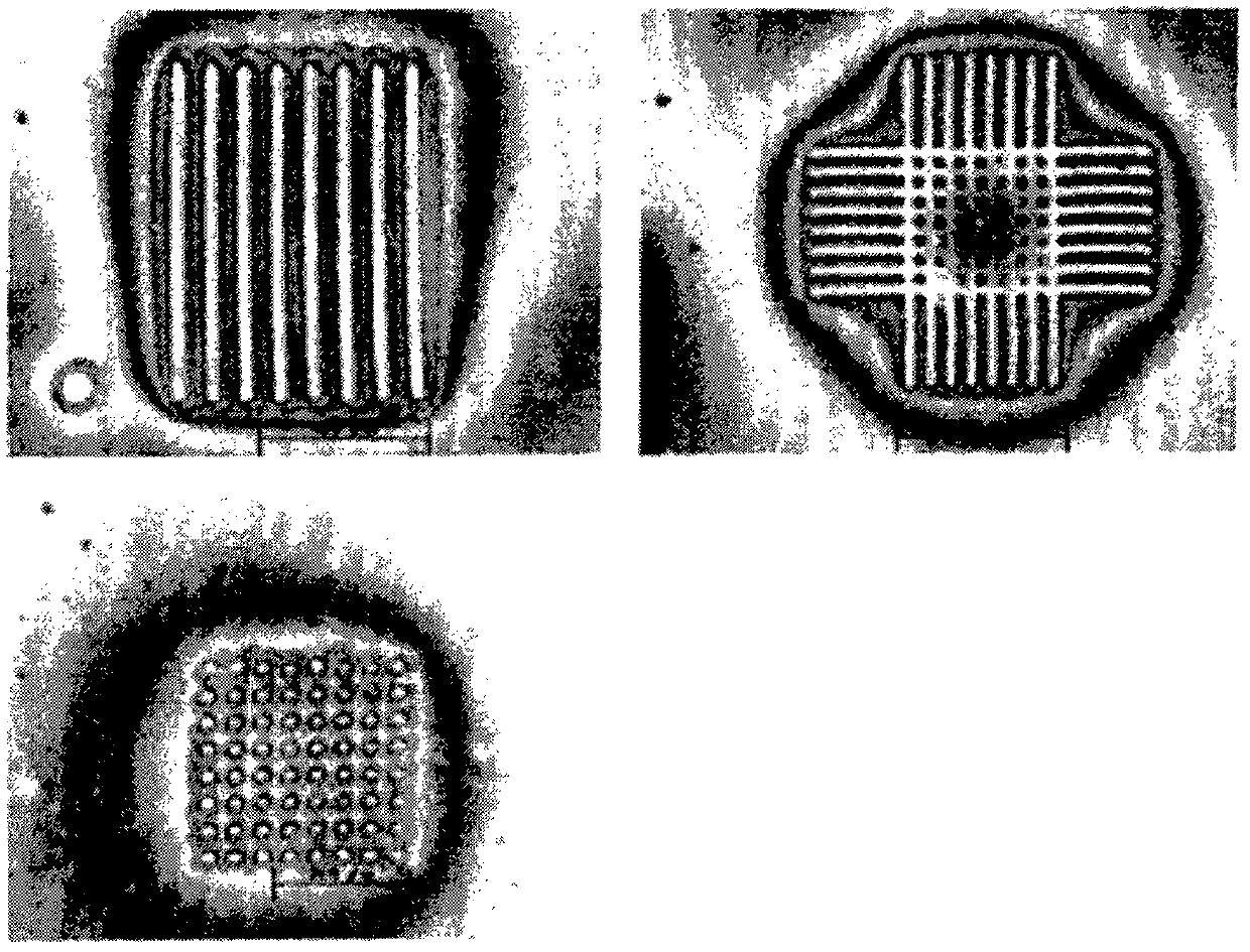
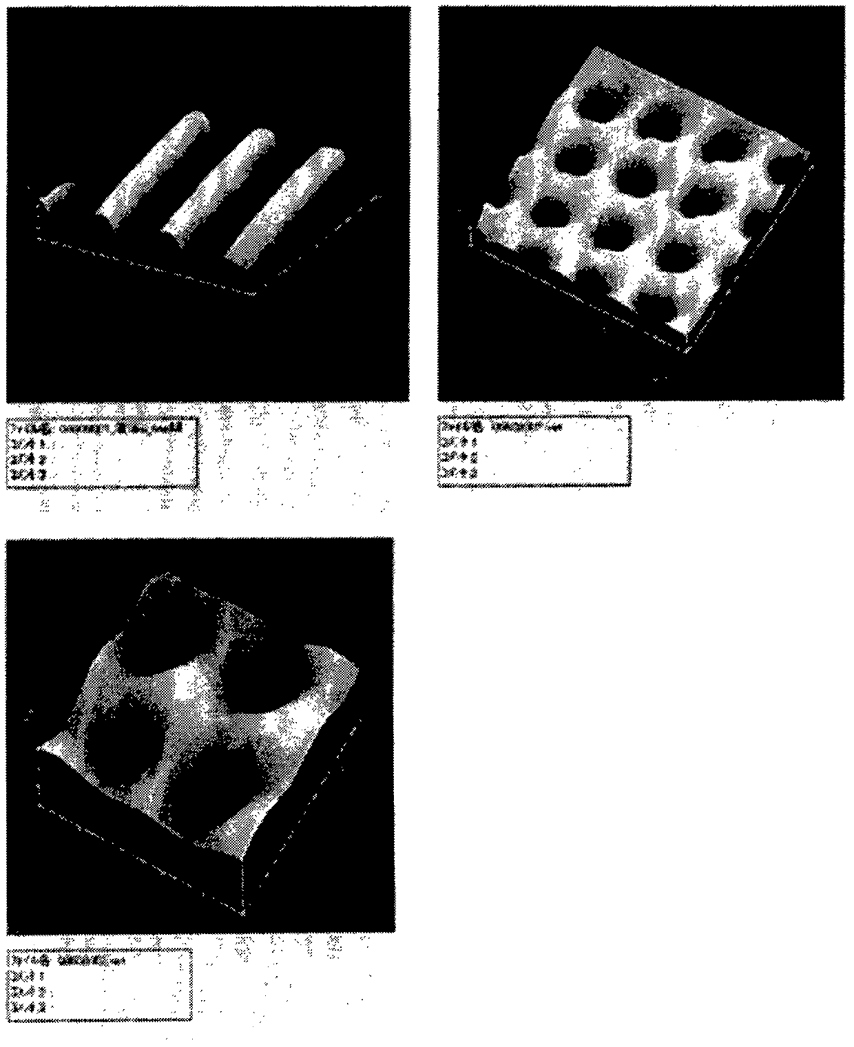
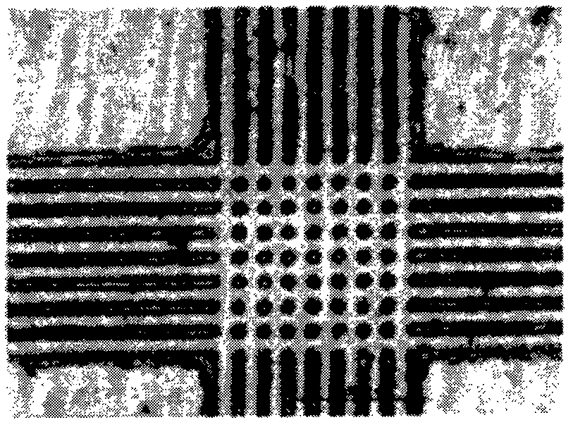
[0120] As the master mold, "PH-350" (trade name, multiple line-space patterns of different line widths with a line width of 0.35 to 3 μm, and different sizes with a diameter of 0.5 to 10 μm) was used as the master mold. A mold for nanoimprint testing with a plurality of cylindrical protrusions and a plurality of angular patterns of different sizes ranging from 0.5 to 10 μm on one side.). Before use, the master mold is coated with a precision mold release agent "Durasurf HD-1100" manufactured by Daikin Chemicals Co., Ltd. by spin coating, and then heated at 60°C for 5 minutes to perform mold release treatment. .

[0121] In addition, a glass substrate was prepared, and the same operation as that of the above-mentioned master mold was performed, and mold release treatment was performed.

[0122] SYLGARD 184 SILICONE ELASTOMER BASE (agent A) and SYLGARD 184 SILICONE ELASTOMER CURING AGENT (B agent), two-component curable polydimethylsiloxane (PDMS) manufactured by Dow Corning To...

Synthetic example 1

[0126] While stirring cyclopentasilane without solvent, irradiate 25mW / cm 2 The ultraviolet light containing the bright line with a wavelength of 390nm was used for 1 hour to carry out the photopolymerization of cyclopentasilane to obtain a high-level silane compound. By dissolving the obtained higher silane compound in cyclooctane, a cyclooctane solution containing 10% by weight of the higher silane compound, ie a higher silane composition, was obtained. The weight-average molecular weight of the higher-order silane compound contained in this higher-order silane composition was 10,000, and the viscosity was 100 mPa·s.

[0127]


PUM

PropertyMeasurementUnit
wavelengthaaaaaaaaaa
viscosityaaaaaaaaaa
thicknessaaaaaaaaaa

Abstract

Disclosed is a pattern formation method comprising: a first step of arranging at least one silane compound selected from the group consisting of silicon hydride compounds and silicon halide compounds in a gap formed between a substrate and a pattern-shaped mold; and a second step of applying at least one treatment selected from a heat treatment and an ultraviolet ray radiation treatment to the arranged silane compound. When the second step is carried out under an inert atmosphere or a reductive atmosphere, a pattern comprising silicon can be formed. When at least a part of the second step is carried out under an oxygen-containing atmosphere, a pattern comprising a silicon oxide can be formed.

Description

technical field [0001] The present invention relates to a pattern forming method. Background technique [0002] In semiconductor elements such as integrated circuits and thin film transistors, patterned silicon films, such as amorphous silicon films, polycrystalline silicon films, and single crystal silicon films, are used. The patterning of the silicon film is usually carried out by forming a silicon film on the entire surface by a vapor phase process such as chemical vapor deposition (Chemical Vapor Deposition, CVD) and then removing unnecessary parts by photolithography. . However, in this method, since a gas-phase process is used, there are problems in that large-scale equipment is required, raw material use efficiency is poor, handling is difficult because the raw material is gas, and a large amount of waste is generated. [0003] On the other hand, silicon oxide films are often used as electrical insulating films, dielectric films, and protective films of semiconduct...

Claims


Application Information

Patent Timeline
Patent Type & Authority Applications(China)
IPC IPC(8): H01L21/208B29C59/02C01B33/02C01B33/027
CPCH01L21/02623H01L21/31H01L21/02656B82Y10/00C23C18/14H01L21/02164B82Y40/00C01P2004/20C01B33/18C01P2004/01C23C18/1279C23C18/1208H01L21/02282C01B33/027G03F7/0002H01L21/02532H01L21/0237C23C18/08C23C18/06C01B33/02C23C18/143Y10T428/24612B29C59/02H01L21/208
Inventor 下田达也松木安生川尻陵增田贵史金田敏彦
Owner JAPAN SCI & TECH CORP
Why Eureka
Try Eureka