
Light emitting device including a passivation layer on a light emitting structure

a light emitting structure and passivation layer technology, applied in the direction of solid-state devices, semiconductor devices for light sources, lighting and heating apparatus, etc., can solve the problems of reducing the light intensity po, deteriorating electric reliability, and inability to ensure sufficient contact area, so as to improve light efficiency, minimize light absorption, and improve light intensity po

Active Publication Date: 2021-03-16
SUZHOU LEKIN SEMICON CO LTD
View PDF16 Cites 2 Cited by
  • Summary
  • Abstract
  • Description
  • Claims
  • Application Information

AI Technical Summary

Benefits of technology

The patent text describes a new light emitting device with improved light intensity and efficiency. It does this by minimizing light absorption by the paste used in the device. Additionally, the device solves the problem of not having enough secure electrical contact between the package body and the bump or other components. The device also includes branched electrodes that further improve efficiency.

Problems solved by technology

On the other hand, according to the related art, the light emitting device chip is mounted on a predetermined package body by using solder paste, and there is a problem that the light intensity Po is lowered by such a solder paste.
Further, according to the related art, when the light emitting device chip is mounted on a predetermined package body using solder paste, it cannot be ensured that the light emitting device chip is sufficiently wide due to the light absorption problem of the solder paste or the like, a sufficient contact area cannot be ensured and electric reliability is deteriorated.
Such branched electrodes absorb light emitted from the light emitting layer, resulting in deterioration of light efficiency.

Method used


Image

  • Light emitting device including a passivation layer on a light emitting structure
  • Light emitting device including a passivation layer on a light emitting structure
  • Light emitting device including a passivation layer on a light emitting structure

Examples


first embodiment

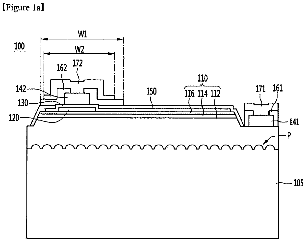
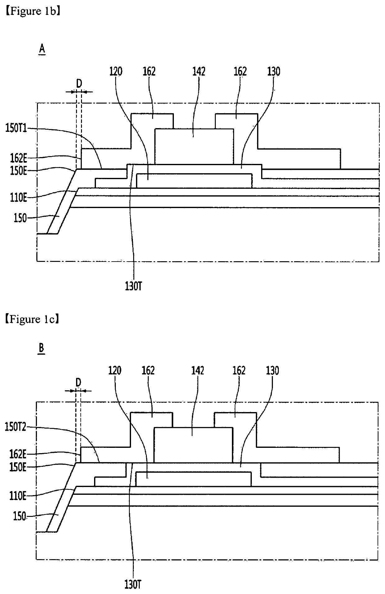
[0069]FIG. 1a is a cross-sectional view of a light emitting device 100 according to the first embodiment.

[0070]The light emitting device 100 according to the embodiment may include at least one of the light emitting structure 110, the substrate 105, the first electrode 141, the second electrode 142, the first insulating reflective layer 161, the second insulating reflective layer 162, a first wetting layer 171, and a second wetting layer 172.

[0071]The light emitting structure 110 may include a first conductivity type semiconductor layer 112, an active layer 114 on the first conductivity type semiconductor layer 112, and a second conductivity type semiconductor layer 116 on the active layer 114.

[0072]For example, the light emitting device 100 according to the embodiment may include a light emitting structure110 including a first conductivity type semiconductor layer 112, an active layer 114 disposed on the first conductivity type semiconductor layer 112, a second conductivity type se...

second embodiment

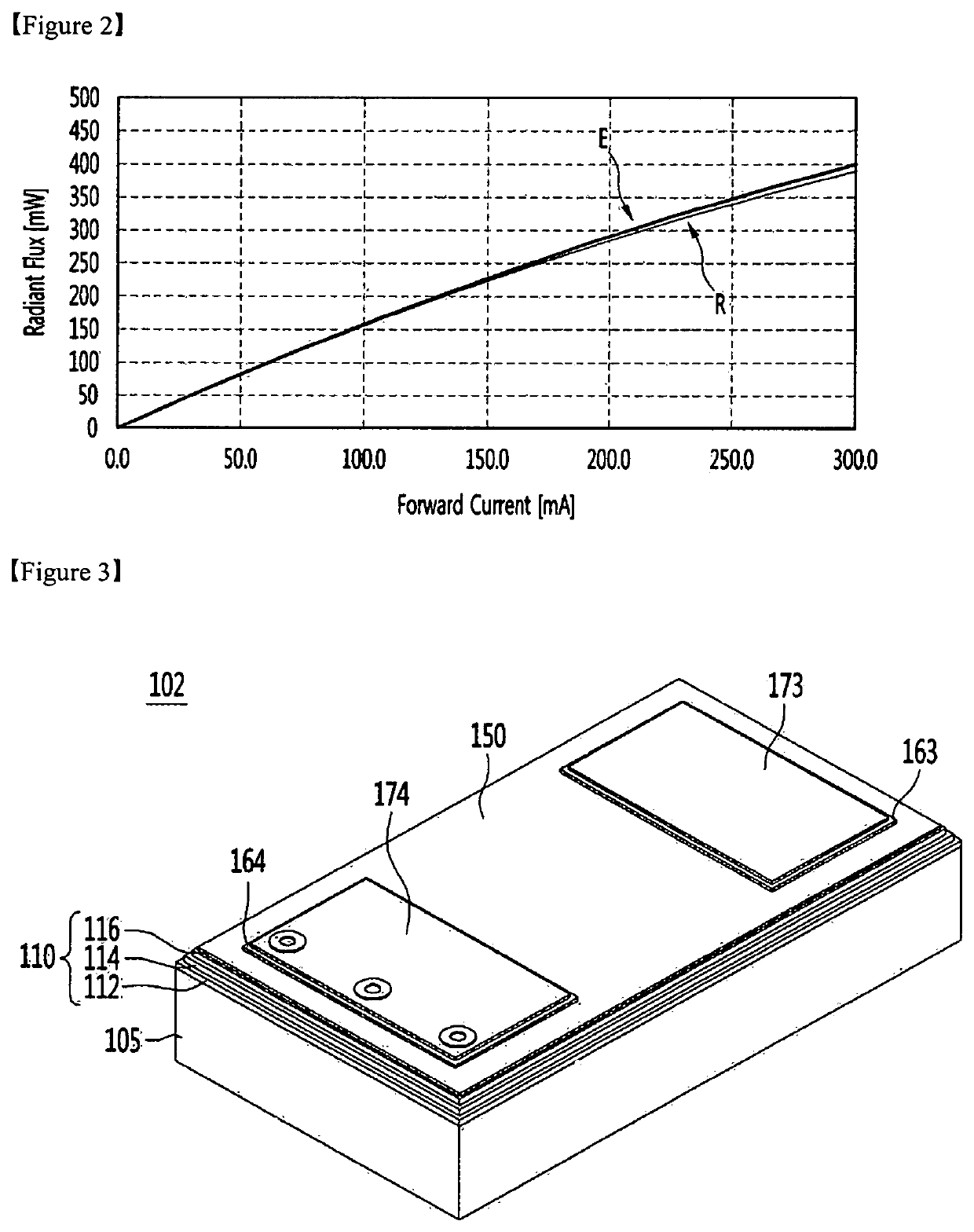
[0168]FIG. 3 is a perspective view of the light emitting device 102 according to the second embodiment, FIG. 4 is a plan projective view of the package 102 of the light emitting device according to the second embodiment, and FIG. 5 is a sectional view taken along the line A-A′ in FIG. 4 in the package 102 of FIG. 4.

[0169]The second embodiment can employ the technical features of the first embodiment, and the following description will focus on the main features of the second embodiment.

[0170]Referring to FIG. 3, the light emitting device 102 according to the second embodiment may include at least one of a substrate 105, a light emitting structure 110, a third insulating reflective layer 163, a fourth insulating reflective layer 164, a third wetting layer a wetting layer 173, a fourth wetting layer 174, and a passivation layer 150.

[0171]For example, referring to FIG. 4, the light emitting device 102 according to the second embodiment may include at least one of a light emitting struc...

third embodiment

[0204]FIG. 6 is a sectional view of the package 102 of the light emitting device according to the third embodiment.

[0205]The light emitting device according to the third embodiment may employ the technical features of the first or second embodiment, and the following description will focus on the main features of the third embodiment.

[0206]The light emitting device according to the third embodiment may include a first reflective layer 181 disposed below the plurality of third electrodes 143 and a second reflective layer 182 disposed below the plurality of fourth electrodes 144.

[0207]The first reflective layer 181 and the second reflective layer 182 may be formed of a metal layer including Al, Ag, or an alloy including Al or Ag.

[0208]According to the third embodiment, although the third electrode 143 is disposed on the light emitting structure 110, the third A electrode 141A and the third B electrode 141B are physically spaced from each other, the third electrode 141A and the third B...


PUM

PropertyMeasurementUnit
wavelength rangeaaaaaaaaaa
reflectivityaaaaaaaaaa
conductivityaaaaaaaaaa

Abstract

The embodiments of the present invention relate to a light emitting device, a method for manufacturing a light emitting device, a light emitting device package, and a lighting device. A light emitting device according to an embodiment has: a light emitting structure including a first conductivity type semiconductor layer, a second conductivity type semiconductor layer, and an active layer disposed between the first conductivity type semiconductor layer and the second conductivity type semiconductor layer; a passivation layer disposed on the light emitting structure; and an insulating reflective layer disposed on the passivation layer. The passivation layer may include a first region disposed on an upper surface of the light emitting structure, and a second region disposed on side surfaces of the first conductivity type semiconductor layer, the second conductivity type semiconductor layer, and the active layer. The insulating reflective layer may be disposed on the first region, and an end portion of the insulating reflective layer may be disposed apart from an end portion of the first region.

Description

CROSS REFERENCE TO RELATED APPLICATIONS[0001]This application is the National Phase of PCT International Application No. PCT / KR2017 / 014261, filed on Dec. 6, 2017, which claims priority under 35 U.S.C. 119(a) to Patent Application No. 10-2016-0164908, filed in the Republic of Korea on Dec. 6, 2016, all of which are hereby expressly incorporated by reference into the present application.TECHNICAL FIELD[0002]Embodiments relate to a light emitting device, a light emitting device package, and a lighting device including the same.BACKGROUND ART[0003]Semiconductor devices including compounds such as GaN and AlGaN have many merits such as wide and easy bandgap energy, and can be used variously as light emitting devices, light receiving devices, and various diodes.[0004]Particularly, a light emitting device such as a light emitting diode or a laser diode using a semiconductor material of Group III-V or II-VI group semiconductors can be applied to various devices such as a Red, Blue, and ultr...

Claims


Application Information

Patent Timeline
Patent Type & Authority Patents(United States)
IPC IPC(8): H01L33/40F21K9/00H01L33/10H01L33/30H01L33/38H01L33/42H01L33/46H01L33/62
CPCH01L33/405F21K9/00H01L33/10H01L33/30H01L33/387H01L33/42H01L33/46H01L33/62H01L33/44H01L33/20H01L2933/0016H01L33/36H01L33/48H01L2924/12041F21Y2115/10
Inventor HWANG, SUNG MINPARK, SUN WOOLEE, CHANG HYEONG
Owner SUZHOU LEKIN SEMICON CO LTD
Learn More