Camera module, dual camera module, optical device, and method for manufacturing dual camera module

a dual camera module and optical device technology, applied in the direction of cameras, printers, instruments, etc., can solve the problems of affecting the other lens driving device, the alignment between the two image sensors becomes twisted, and the process defect rate is reduced, and the alignment quality of image sensors can be improved. , the effect of improving the alignment change of image sensors relative to impact and temperatur

Active Publication Date: 2021-04-06
LG INNOTEK CO LTD
View PDF29 Cites 2 Cited by
  • Summary
  • Abstract
  • Description
  • Claims
  • Application Information

AI Technical Summary

Benefits of technology

[0136]A process defect rate may be reduced through a first exemplary embodiment of the present invention by allowing an alignment to be enabled after an image sensor is mounted. An alignment quality of image sensors can be improved over the conventional method. An alignment change of image sensors relative to impact and temperature can be improved. To be more specific, although a PCB flatness change to impact and temperature is conventionally ensued to alignment change of image sensors, the alignment of image sensors can be adjusted even if there is a PCB flatness change according to the present exemplary embodiment.
[0137]A magnetic influence mutually affected by magnets of two camera modules in a dual camera module can be minimized through a second exemplary embodiment of the present invention. Through this advantageous effect, a discrete distance between two camera modules can be minimized.
[0138]A distance between a filter disposed on a sensor base and a lens driving device disposed on a top surface of sensor base may be secured through a third exemplary embodiment of the present invention. Through this advantageous effect, an AA (Active Alignment) space for lens focusing can be secured. Furthermore, shock reliability can be secured by improvement in filter breakage. A flare phenomenon can be minimized through the third exemplary embodiment. To be more specific, a phenomenon in which a light bounced off from a gold wire and a passive element is re-incident on a lens side can be minimized. A cost reduction can be expected by non-application of black mask disposed on a filter in order to inhibit the conventional flare phenomenon.
[0139]A phenomenon in which a lens driving device is disengaged from a sensor base during drop test and tumble test can be inhibited through a fourth exemplary embodiment of the present invention.

Problems solved by technology

The conventional dual camera module suffers from disadvantages in that there is no way to adjust two image sensors subsequent to alignment thereof after the two image sensors are mounted on a PCB (Printed Circuit Board) and the alignment between the two image sensors becomes twisted due to heat or shock.
Moreover, when two lens driving devices are proximately arranged for obtainment of good performance of dual camera, a magnetic force of a magnet on any one lens driving device of two lens driving devices problematically affects the other lens driving device.
Still another problem is that a distance between an upper end of an image sensor and a lower end of lens may be shortened in a camera module depending on design, and in this case, a wire applying a power to the image sensors and the PCB may problematically interfere with a sensor base.
However, unlike the increased diameter of lens and the lens barrel, an adhesive area between a lens driving device and a sensor base becomes relatively decreased to disadvantageously generate the disengagement of lens driving device during drop test or tumble test.

Method used


Image

  • Camera module, dual camera module, optical device, and method for manufacturing dual camera module
  • Camera module, dual camera module, optical device, and method for manufacturing dual camera module
  • Camera module, dual camera module, optical device, and method for manufacturing dual camera module

Examples


first exemplary embodiment

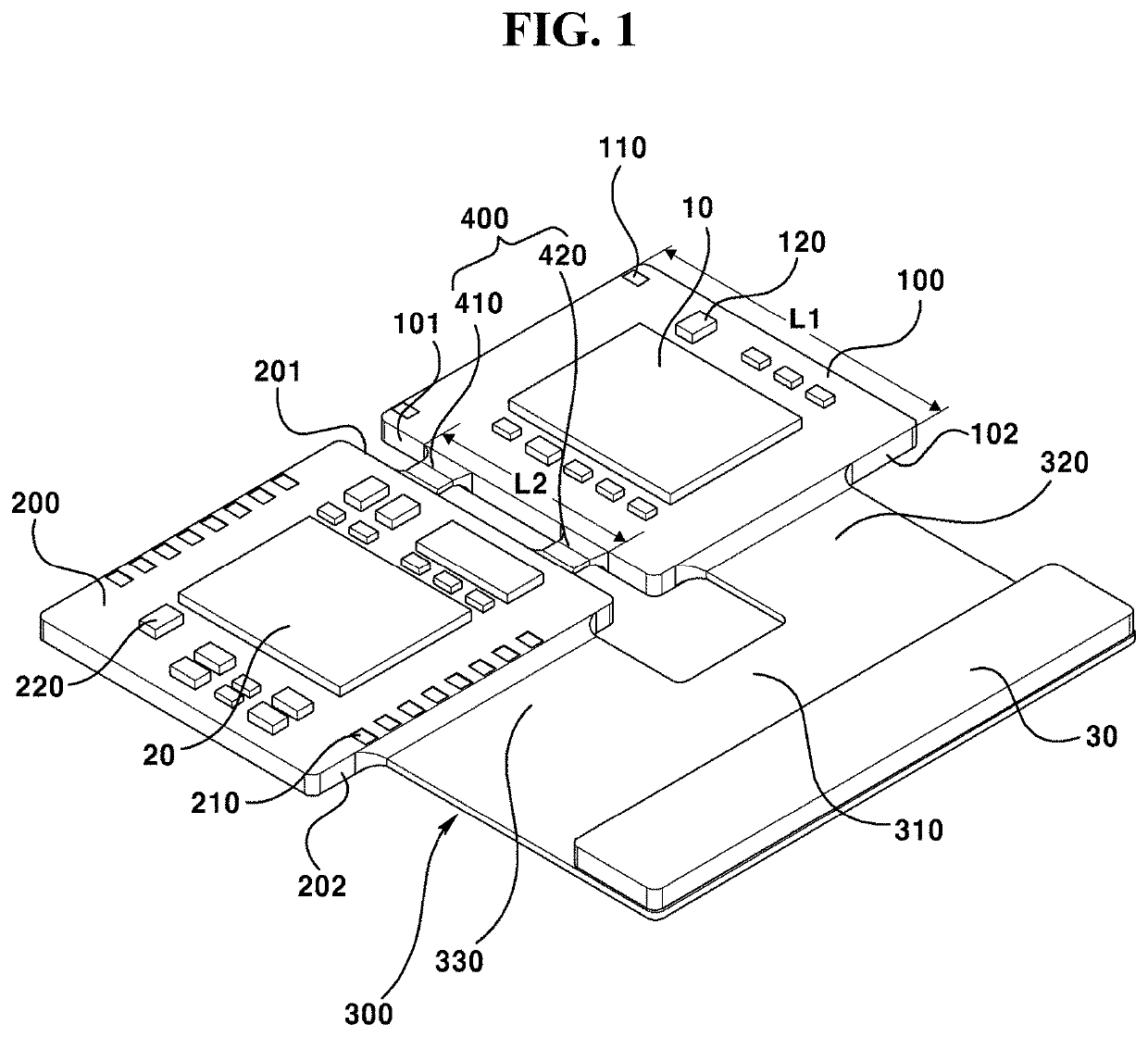
[0202]Now, configuration of optical device according to a first exemplary embodiment will be described.

[0203]An optical device may be any one of a hand phone, a mobile phone, a smart phone, a portable smart device, a digital camera, a notebook computer (laptop computer), a digital broadcasting terminal, a PDA (Personal Digital Assistant), a PMP (Portable Multimedia Player) and a navigation device. However, the present invention is not limited thereto, and the optical device may comprise any device capable of capturing an image or a photograph.

[0204]The optical device may comprise a main body (not shown), a dual camera module and a display part (not shown). However, any one or more of the elements in the main body, the dual camera module and the display part may be omitted or changed from the optical device.

[0205]The main body may form an external shape of an optical device. The main body may comprise a cubic shape, for example. However, the present invention is not limited thereto. ...

second exemplary embodiment

[0381]Hereinafter used “OIS feedback function” is defined as a function to feedback-control the OIS function in real time. Meantime, the “OIS feedback” may be interchangeably used with an “OIS Feedback”. Hereinafter used “first AF feedback sensor (3710)” may be called a “first Hall sensor”, and a “second AF feedback sensor (4710)” may be called a “second Hall sensor”.

[0382]Hereinafter, an optical device according to a second exemplary embodiment may be inferably applied with the optical device according to the first exemplary embodiment.

[0383]Hereinafter, configuration of dual camera module according to a second exemplary embodiment will be described with accompanying drawings.

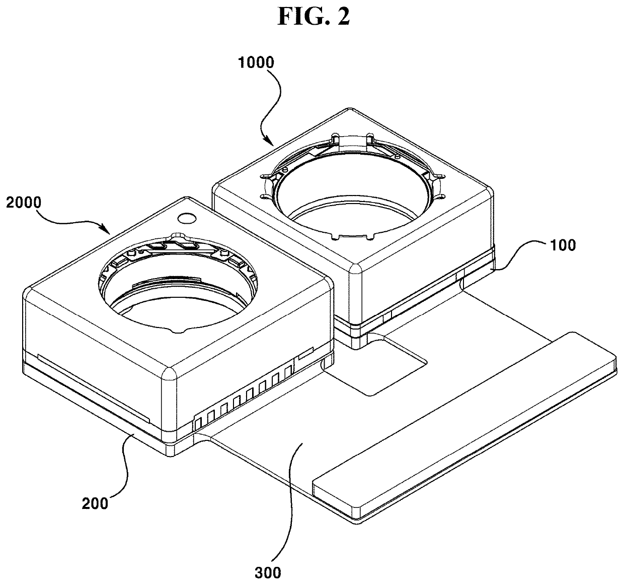
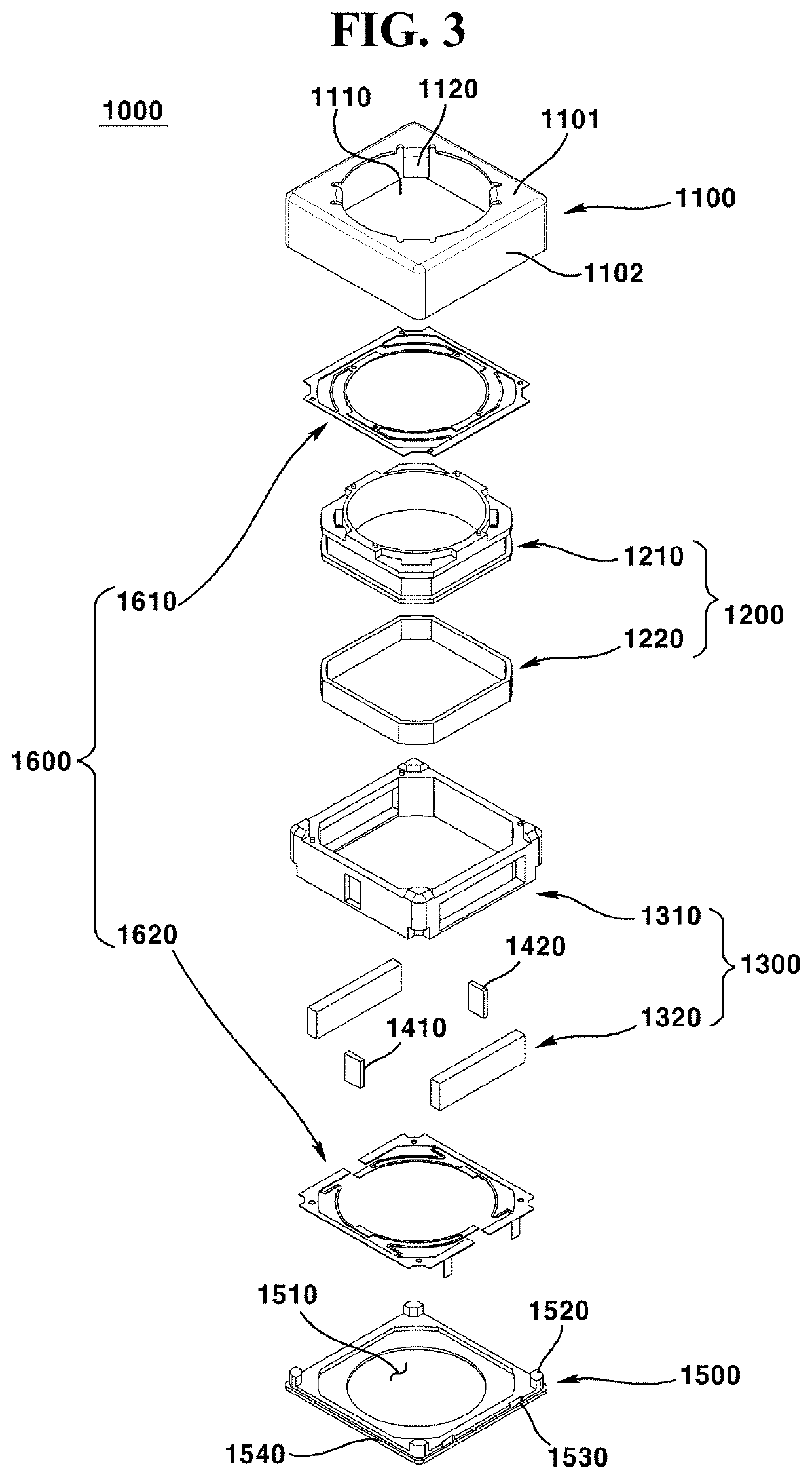
[0384]FIG. 15 is a perspective view illustrating a dual camera module according to a second exemplary embodiment.

[0385]The dual camera module according to the second exemplary embodiment may comprise a first camera module and a second camera module. The dual camera module according to the second exemplary embo...

third exemplary embodiment

[0585]Hereinafter, configuration of optical device according to a third exemplary embodiment will be described with reference to the accompanying drawing.

[0586]FIG. 42 is a perspective view of an optical device according to a third exemplary embodiment.

[0587]The optical device may be any one of a hand phone, a mobile phone, a smart phone, a portable smart device, a digital camera, a notebook computer (laptop computer), a digital broadcasting terminal, a PDA (Personal Digital Assistant), a PMP (Portable Multimedia Player) and a navigation device. However, the present invention is not limited thereto, and may comprise any device capable of capturing an image or a photograph.

[0588]The optical device may comprise a main body (5001), a display part (5002) and a camera module (5003). However, any one or more of the main body (5001), the display part (5002) and the camera module (5003) may be omitted or changed from the optical device.

[0589]The main body (5001) may form an external shape o...


PUM

PropertyMeasurementUnit
distanceaaaaaaaaaa
distanceaaaaaaaaaa
distanceaaaaaaaaaa

Abstract

The present embodiment relates to a dual camera module comprising: a rigid first substrate having a first image sensor arranged thereon; a rigid second substrate spaced apart from the first substrate and having a second image sensor arranged thereon; a third substrate connected to the first substrate and the second substrate; and a flexible connection unit for connecting the first substrate to the second substrate, wherein the first substrate includes a first side surface, the second substrate includes a second side surface facing the first side surface, and the connection unit connects the first side surface of the first substrate to the second side surface of the second substrate.

Description

CROSS-REFERENCE TO RELATED APPLICATIONS[0001]This application is the U.S. national stage application of International Patent Application No. PCT / KR2017 / 012285, filed Nov. 1, 2017; which claims the benefit under 35 U.S.C. § 119 of Korean Application Nos. 10-2016-0144381, filed Nov. 1, 2016; 10-2017-0002960, filed Jan. 9, 2017; 10-2017-0004206, filed Jan. 11, 2017; and 10-2017-0018832, filed Feb. 10, 2017; all of which are hereby incorporated by reference in their entirety.TECHNICAL FIELD[0002]The teachings in accordance with exemplary and non-limiting embodiments of this invention relate generally to a camera module, a dual camera module, an optical device and a method for manufacturing a dual camera module.BACKGROUND ART[0003]This section provides background information related to the present invention, which is not necessarily prior art.[0004]Concomitant with generalization of wide use of various mobile terminals, and commercialization of wireless internet services, demands by cons...

Claims


Application Information

Patent Timeline
Patent Type & Authority Patents(United States)
IPC IPC(8): G03B17/12G03B17/02G03B19/22H04N5/225H01F7/08H01F7/16H04N5/232H04N5/247H04N5/335
CPCG03B17/12G03B17/02G03B19/22H01F7/08H01F7/16H04N5/225H04N5/2251H04N5/2252H04N5/232H04N5/247H04N5/335G03B30/00H04N23/00H04N23/45H04N23/50H04N25/00G03B2205/0069G03B3/10G03B5/00H04N23/54H04N23/51H04N23/60H04N23/90
Inventor PARK, SANG OKKIM, TAE YOUNGOH, HYUN AHJEONG, YOUN BAEK
Owner LG INNOTEK CO LTD
Why Eureka
Try Eureka