Broadband meta-optical device

a meta-optical device and broadband technology, applied in optics, instruments, optical elements, etc., can solve the problems of not being able to achieve wavelength division multiplexing nor display in three primary colors, not performing so well for resonances with other wavelengths, and poor image quality, so as to achieve a wide operating wavelength range, shorten the wavelength spectrum, and increase the effect of plasma resonan

Active Publication Date: 2021-08-10
ACAD SINIC
View PDF3 Cites 1 Cited by
  • Summary
  • Abstract
  • Description
  • Claims
  • Application Information

AI Technical Summary

Benefits of technology

[0008]To enable optical components based on nanoplasmonic structures to be further applied to applications with shorter wavelengths and achieve display in three primary colors, an object of the present invention is to provide an optical component including: a dielectric layer and a primary nanorod array formed thereon. The primary nanorod array is formed on the dielectric layer to define a pixel, and is composed of a plurality of nanorod sub-arrays arranged in two-dimensional arrays. Each nanorod sub-array is composed of a plurality of nanorods arranged in two-dimensional arrays, and the nanorods within a same nanorod sub-array are rectangular rods of the same shape. Each nanorod has a width and a length, and the length direction serves as the direction of that nanorod. All the nanorods within a single nanorod sub-array have the same length and are of the same direction. Moreover, among the plurality of nanorod sub-arrays which belong to a single pixel, at least three nanorod sub-arrays are composed of nanorods having different lengths. The single pixel includes at least two nanorod sub-arrays along a width direction thereof, and at least two nanorod sub-arrays along a length direction thereof. The nanorods are made of metal which has a relatively higher plasma resonance, so that a broader operating wavelength range can be achieved to cover shorter wavelengths of the spectrum.

Problems solved by technology

However, it does not perform so well for resonances with other wavelengths, and cannot achieve wavelength division multiplexing nor display in three primary colors.
Although a different kind of dielectric metasurface aiming to improve the above-described lenses has been proposed, chromatic aberrations, which can result in poor image quality, remain a problem for such metasurfaces.

Method used


Image

  • Broadband meta-optical device
  • Broadband meta-optical device
  • Broadband meta-optical device

Examples


Embodiment Construction

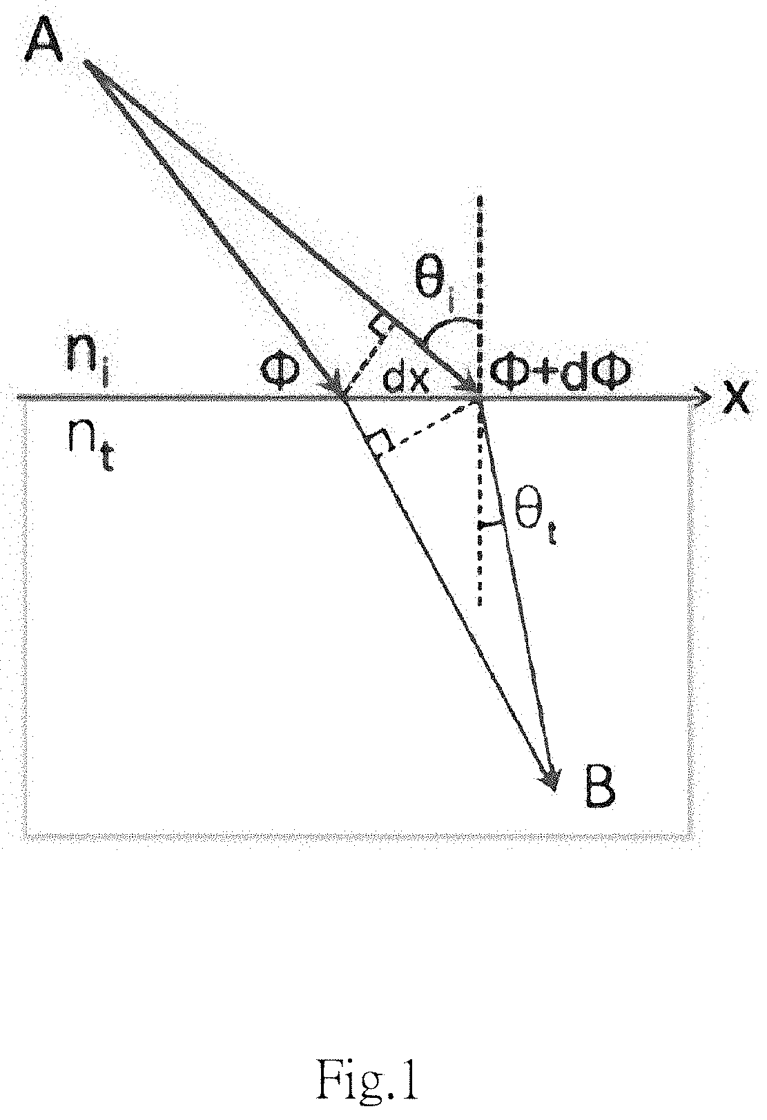
[0031]The nanoscale optical component exemplified in the present invention is a type of metasurface. In general, such metasurface has a plurality of metal nanostructures periodically arranged thereon, and the design and arrangement of those metal nanostructures are mostly related to phase modulation for electromagnetic waves. When an incident electromagnetic wave arrives at the metasurface, the metal nanostructure thereof is then excited and a plasmon resonance occurs, which causes the metal nanostructure to further radiate an electromagnetic wave. Compared to the incident wave, the radiated electromagnetic wave from the excited metal nanostructure has been altered in intensity and phase and is propagating in accordance with the generalized Snell's Law.

[0032]Generalized Snell's Law

[0033]With reference to FIG. 1, as far as a metasurface is concerned, an artificial structure (such as the metal nanostructure according to the present invention) configured on an interface defined between...


PUM

PropertyMeasurementUnit
thickness H1aaaaaaaaaa
thickness H2aaaaaaaaaa

Abstract

The present invention provides an optical component comprising a dielectric layer and a nanorod array; the nanorod array is formed on a surface of the dielectric layer and extends along a lateral direction and a vertical direction. The nanorod array comprises a plurality of nanorods extending along the dielectric layer. The nanorods have a gap between one another, and an angle is defined by two adjacent nanorods. A bump is formed at each of two ends of the nanorod.

Description

BACKGROUND OF THE INVENTIONField of the Invention[0001]The present invention relates to an optical component / device, and more particularly, to a phase-modulated optical component / device using plasmonic coupling induced by nano-structure.Description of the Prior Art[0002]Optical components made of plasmonic metamaterials relate to the technical fields of nanomaterials and nanophotonics. Basically, a plasmonic metamaterial utilizes the anomalous optical phenomenon which is generated when resonance occurs for the electrons in a metal nanostructure. Particular applications of plasmonic metamaterials include realizations of, for example, negative index materials, superlenses, phase modulation, holograms, etc.[0003]For example, plasmonic metasurfaces utilize custom unit element with sub-wavelength nanostructures on metasurfaces to modulate the phase of incident light (i.e., the electromagnetic wave), so that wavefronts of electromagnetic waves can be altered.[0004]For further example, a p...

Claims


Application Information

Patent Timeline
Patent Type & Authority Patents(United States)
IPC IPC(8): G02B5/00G02B1/00G03H1/02G03H1/08
CPCG02B5/008G02B1/002G03H1/0244G03H1/0891G02F1/0054
Inventor TSAI, DIN-PINGWU, PIN-CHIEH
Owner ACAD SINIC
Why Eureka
Try Eureka