Plasma CVD apparatus, method for manufacturing microcrystalline semiconductor layer, and method for manufacturing thin film transistor

Inactive Publication Date: 2009-02-19
SEMICON ENERGY LAB CO LTD
View PDF38 Cites 22 Cited by
  • Summary
  • Abstract
  • Description
  • Claims
  • Application Information

AI Technical Summary

Benefits of technology

[0013]In the present invention, two or more high-frequency electric powers with different frequencies are supplied to an electrode for producing glow discharge plasma, which is provided in a reaction chamber. The high-frequency electric power is an alternating-current power. The high-frequency electric powers with different frequencies are supplied to produce glow discharge plasma, so that a thin film including a semiconductor or an insulating material is formed. One of the high-frequency electric powers (a first high-frequency electric power) is an electric power in a frequency band where the surface standing wave effect does not appear, and a high frequency with a wavelength of about 10 m or more is applied. In addition, a second high-frequency electric power has a shorter wavelength, that is, a higher frequency, than the first high-frequency electric power, and the second high-frequency electric power is added to the first high-frequency electric power.
[0014]An aspect of the present invention is to enable switching of the following cases freely when an insulating layer and a semiconductor layer for forming a TFT are manufactured. One of the cases is that two or more high-frequency electric powers with different frequencies are supplied to an electrode for producing glow discharge plasma, which is provided in a reaction chamber. The other case is that one high frequency electric power with a frequency is supplied thereto. When glow discharge plasma is produced by supplying the high-frequency electric powers with different frequencies, one of the high-frequ

Problems solved by technology

However, polycrystalline silicon needs to be subjected to excimer laser annealing, and a production line for manufacturing an amorphous silicon TFT needs to be drastically changed.
Thus, newly capital investment is necessary, and the polycrystalline silicon TFT panels cannot compete against amorphous silicon TFT panels in the production cost.
On the other hand, the amorphous silicon TFTs have difficulty in solving such a pro

Method used


Image

  • Plasma CVD apparatus, method for manufacturing microcrystalline semiconductor layer, and method for manufacturing thin film transistor
  • Plasma CVD apparatus, method for manufacturing microcrystalline semiconductor layer, and method for manufacturing thin film transistor
  • Plasma CVD apparatus, method for manufacturing microcrystalline semiconductor layer, and method for manufacturing thin film transistor

Examples


embodiment mode 1

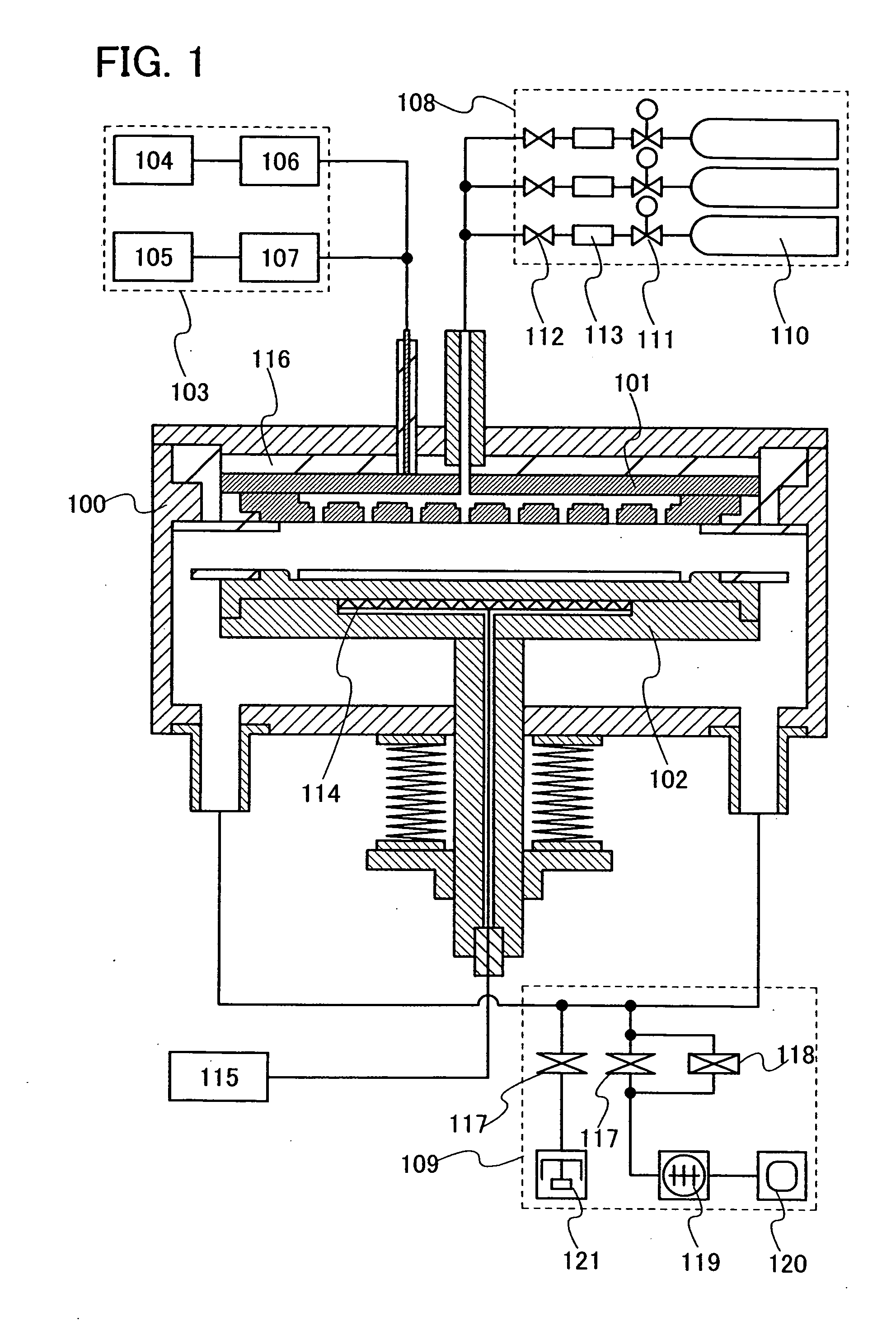
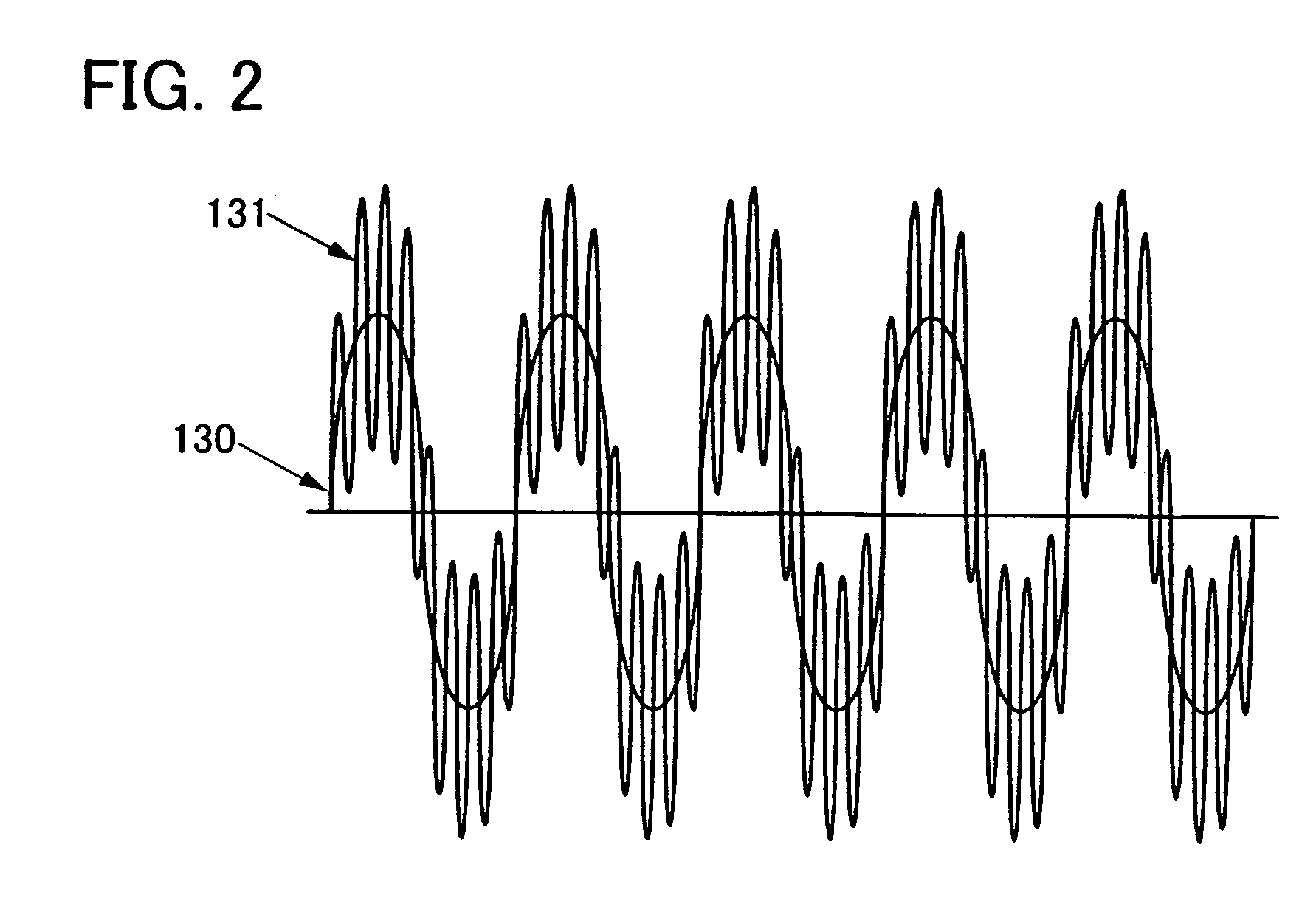
[0049]FIG. 1 illustrates an example of a structure of a plasma CVD apparatus where high-frequency electric powers with different frequencies are applied. A reaction chamber 100 is formed of a material having rigidity, such as aluminum or stainless, and has a structure in which the inside can be evacuated to vacuum. In the reaction chamber 100, a first electrode 101 and a second electrode 102 are provided. The first electrode 101 and the second electrode 102 are disposed to face each other.

[0050]A high-frequency power supply means 103 is connected to the first electrode 101. The ground potential is supplied to the second electrode 102 which has such a shape that a substrate can be mounted. The first electrode 101 is insulated from the reaction chamber 100 with an insulating material 116, so that the high-frequency electric power does not leak. Although the first electrode 101 and the second electrode 102 have a capacitive coupled (parallel plate) structure in FIG. 1, another structur...

embodiment mode 2

[0078]This embodiment mode will exemplify a structure of a plasma CVD apparatus suitable for formation of a gate insulating layer and a semiconductor layer included in a TFT, as an example of the plasma CVD apparatus that employs the reaction chamber shown in Embodiment Mode 1.

[0079]FIG. 6 illustrates an example of a multi-chamber plasma CVD apparatus provided with a plurality of reaction chambers. This apparatus has a common chamber 123, a load / unload chamber 122, a first reaction chamber 100a, a second reaction chamber 100b, and a third chamber 100c. The plasma CVD apparatus has a single-wafer structure in which substrates loaded in a cassette 124 in the load / unload chamber 122 are carried in and out of each chamber by a transport mechanism 126 of the common chamber 123 one by one. Gate valves 125 are provided between the common chamber 123 and each chamber, so that treatment conducted in the chambers does not interfere with each other.

[0080]Each reaction chamber is used for a dif...

embodiment mode 3

[0086]This embodiment mode will exemplify an example of a method for manufacturing a TFT, provided in a pixel in a display device, in which a channel formation region is formed using a microcrystalline silicon layer with use of the plasma CVD apparatus described in Embodiment Mode 1 and Embodiment Mode 2.

[0087]FIG. 8, FIG. 9, FIG. 10, and FIG. 11 are plane views of a pixel, and FIG. 12, FIG. 13, FIG. 14, FIG. 15, and FIG. 16 are cross-sectional views taken along lines A-B of the plane views. Hereinafter, description is made with reference to these plane views and cross-sectional views as appropriate.

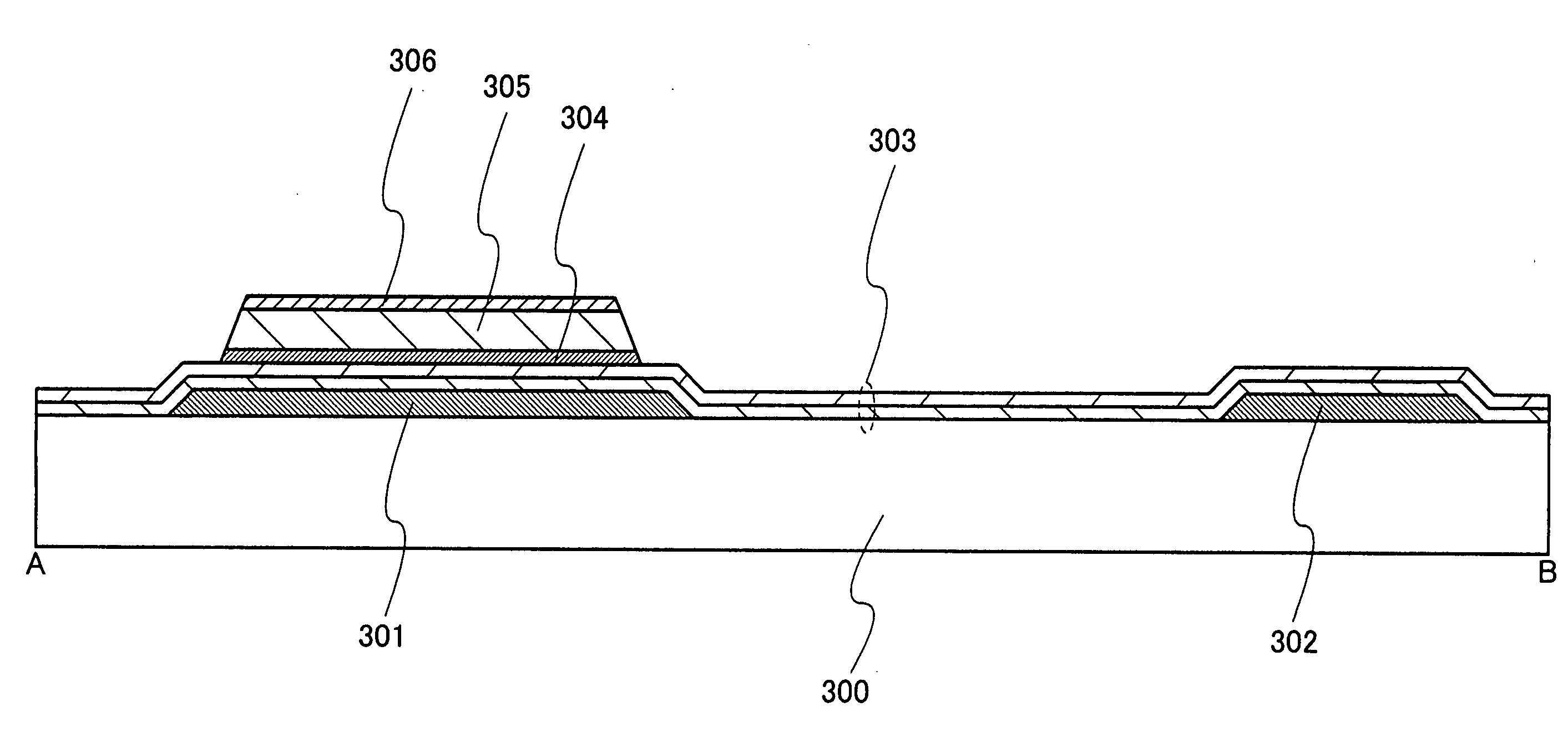
[0088](1) Formation of Gate Electrode and Capacitor Electrode

[0089]A flat-plate substrate having an insulating surface, such as a glass substrate, is applied as an element substrate 300 over which a TFT is manufactured. A gate electrode 301 and a capacitor electrode 302 are formed over the element substrate 300 (see FIG. 8 and FIG. 12).

[0090]The gate electrode 301 and the capacitor elect...


PUM

PropertyMeasurementUnit
Lengthaaaaaaaaaa
Lengthaaaaaaaaaa
Frequencyaaaaaaaaaa

Abstract

As an electrode area of a plasma CVD apparatus is enlarged, influence of the surface standing wave remarkably appears, and there is a problem in that in-plane uniformity of quality and a thickness of a thin film formed over a glass substrate is degraded. Two or more high-frequency electric powers with different frequencies are supplied to an electrode for producing glow discharge plasma in a reaction chamber. With glow discharge plasma produced by supplying the high-frequency electric powers with different frequencies, a semiconductor thin film or an insulating thin film is formed. High-frequency electric powers with different frequencies (different wavelengths), which are superimposed on each other, are applied to an electrode in a plasma CVD apparatus, so that increase in plasma density and uniformity for preventing effect of surface standing wave of plasma are attained.

Description

BACKGROUND OF THE INVENTION[0001]1. Field of the Invention[0002]The present invention relates to a technique for forming a thin film and a technique for manufacturing an element utilizing plasma.[0003]2. Description of the Related Art[0004]The market of liquid crystal displays using thin film transistors (hereinafter, also referred to as “TFT”) has been expanded. TFTs are one kind of field effect transistors and include a thin film of a semiconductor layer for forming a channel formation region. The semiconductor layer is formed of amorphous silicon or polycrystalline silicon.[0005]Amorphous silicon TFTs have a problem that time for writing to a pixel is insufficient with increase in a panel size and density of the pixel. It has been considered that polycrystalline silicon TFTs solve the above-mentioned problem because the polycrystalline silicon TFTs have higher electron field-effect mobility than the amorphous silicon TFTs (for example, refer to Patent Document 1: Japanese Publish...

Claims


Application Information

Patent Timeline
IPC IPC(8): H01L21/36C23C16/513H01L21/00
CPCC23C16/509H01L21/02661H01J37/32091H01J37/32165H01J37/32541H01L21/67207H01L29/04H01L29/41733H01L29/4908H01L29/66765H01L29/78696H01L21/02422H01L21/02488H01L21/02532H01L21/0262C23C16/545H01L29/458
Inventor YAMAZAKI, SHUNPEI
Owner SEMICON ENERGY LAB CO LTD
Why Eureka
Try Eureka