
LED backlight device and display device

a backlight device and led backlight technology, applied in semiconductor devices, optics, instruments, etc., can solve the problems of affecting the overall reflection efficiency, affecting the luminous efficiency of the mini led display, and an inevitable loss of light energy, so as to reduce process deviation, improve the design of metal traces, and effectively optimize the manufacturing process

Active Publication Date: 2021-08-17
WUHAN CHINA STAR OPTOELECTRONICS TECH CO LTD
View PDF21 Cites 0 Cited by
  • Summary
  • Abstract
  • Description
  • Claims
  • Application Information

AI Technical Summary

Benefits of technology

This design enhances manufacturing yield, reduces light energy loss, and improves light efficiency by maximizing the coverage of reflective materials and minimizing light transmission through the substrate.

Problems solved by technology

However, the mini LED direct-lit backlight uses a huge number of LEDs in an array, although the LEDs themselves and the bonding pads of LEDs constitute a large area ratio of non-reflector, and the gaps between LEDs are usually covered with high reflectance white solder resist or other highly reflective materials, but the overall reflection efficiency is still lower than the entirely surface reflector of edge-lit backlight structure, so that affects the overall reflection efficiency.
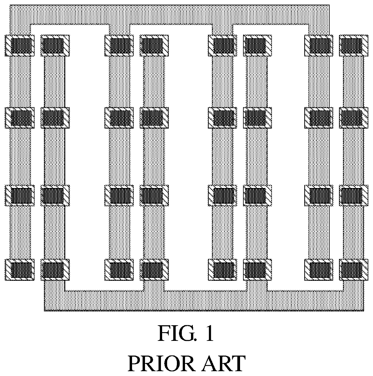
A blank gap may exist between the reflective material and the pads, and the reflective material may cover pads disposed on p / n junctions of the mini LED, which affects electrical properties.
If the deviations are considered in advance, it would make that the blank gap existing between the reflective material and the pad becomes larger, results in the poor luminous efficiency of the mini LED display and an inevitable loss of light energy.
Moreover, the size of mini LED is comparatively small, and it still has problems such as solder paste printing and die-bonding even if the deviation is considered in advance.
The above-mentioned problems cannot be solved simply by improving etching precision in each process.

Method used


Image

  • LED backlight device and display device
  • LED backlight device and display device
  • LED backlight device and display device

Examples


Embodiment Construction

[0059]The following description of embodiments combined with the accompanying drawings is provided to illustrate the specific embodiments of the present invention. The directional terms mentioned in the present invention, such as “upper”, “lower”, “front”, “back”, “left”, “right”, “top”, “bottom”, etc., are only directions by referring to the accompanying drawings, and thus the used directional terms are used to describe and understand the present invention, but the present invention is not limited thereto.

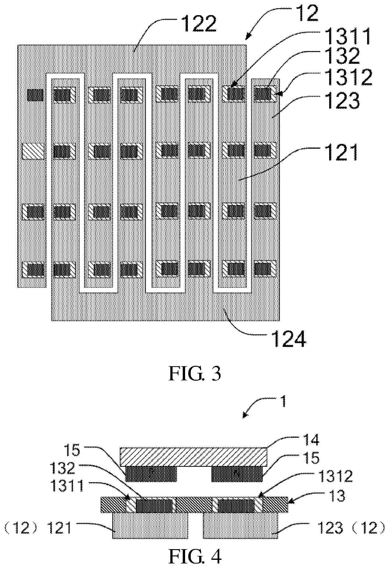
[0060]As shown in FIG. 4, in an embodiment according to present invention, a light emitting diode (LED) backlight device 1 includes a backlight substrate 11, metal traces 12, a reflective material layer 13, a plurality of LED chips 14 and pads 15.

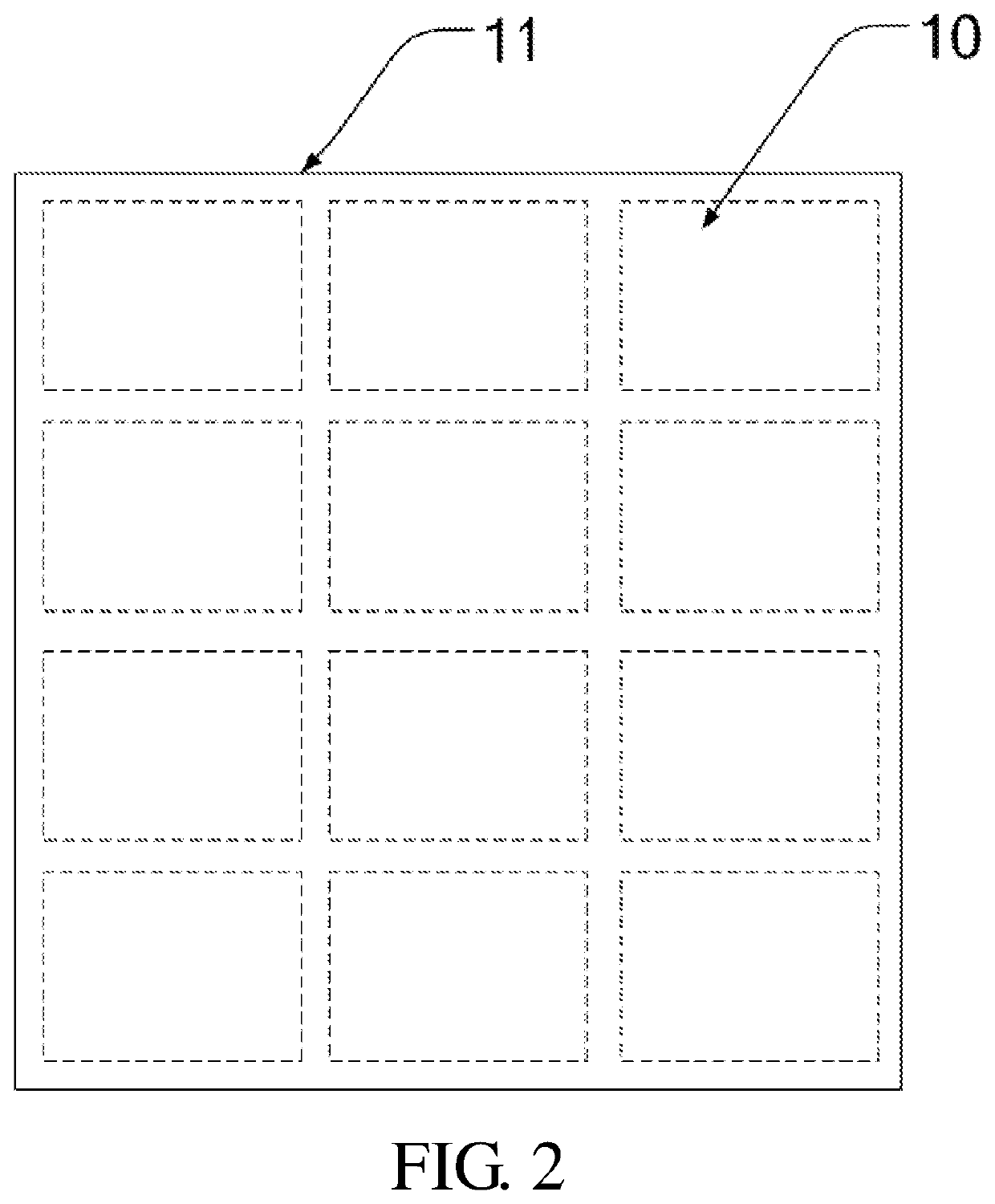
[0061]As shown in FIG. 2, the backlight substrate 11 is provided with a plurality of backlight partitions 10, and the size and number of the backlight partitions 10 are specifically designed according to the actual size parameter of the b...


PUM

PropertyMeasurementUnit
widthaaaaaaaaaa
distanceaaaaaaaaaa
sizeaaaaaaaaaa

Abstract

The present invention discloses a light emitting diode (LED) backlight device and LED display device, including a plurality of backlight partitions; a reflective material layer covering a surface of the backlight substrate; a plurality of metal traces disposed within the backlight partitions and disposed between the backlight substrate and the reflective material layer; a plurality of pad openings penetrating from a surface of the reflective material layer to a surface of the metal traces. An orthographic projection of the pad openings projected toward the backlight substrate is completely within an area of the metal traces; and a plurality of solder paste application regions located in the pad openings. The LED display device assembled by the LED backlight device according to the present invention improves the yield of solder paste printing and die bonding, improves the light reflection, reduces the loss of light energy, and improves the light efficiency.

Description

FIELD OF INVENTION[0001]The present invention relates to display devices, particularly to a field of mini LEDs and the like, and more particularly to a LED backlight device and a LED display device.BACKGROUND OF INVENTION[0002]With rise of wearable application devices such as smart glasses, smart watches and the like, display industry demand for flexible display devices is also increasing. Organic light emitting diode (OLEDs) display has characteristics such as being self-luminous without a backlight source, thin thickness, wide viewing angles, and fast response times, so that it has an inherent advantages for flexible display. Confronted with competition of flexible OLEDs, traditional liquid crystal display technology progressively uses flexible substrates toward the breakout directions such as flexibility and curved surface and the like. It can be seen that an age of flexible and curved display is coming.[0003]Mini LED, also known as “sub-millimeter light-emitting diode”, refers t...

Claims


Application Information

Patent Timeline
Patent Type & Authority Patents(United States)
IPC IPC(8): G02F1/00G02F1/1335G02F1/13357
CPCG02F1/133612G02F1/133603G02F1/133605H01L25/0753H01L33/46H01L33/60H01L33/62
Inventor MA, CHANGWENZHA, GUOWEIZHANG, ZHOU
Owner WUHAN CHINA STAR OPTOELECTRONICS TECH CO LTD
Learn More