Inlet/outlet structure of microfluidic chip and method for sealing same

a microfluidic chip and inlet/outlet structure technology, applied in the field of inlet/outlet structure of a microfluidic chip and a microfluidic chip, can solve the problems of fluid vaporization and loss, large amount of expensive reagents used, and improve the accuracy and deviation of the reaction result, so as to improve the reliability, the effect of less contamination of a fluid sampl

Active Publication Date: 2021-09-07
NANOBIOSYS
View PDF7 Cites 0 Cited by
  • Summary
  • Abstract
  • Description
  • Claims
  • Application Information

AI Technical Summary

Benefits of technology

[0024]The present disclosure provides an inlet / outlet structure optimized for sealing an inlet and an outlet of a microfluidic chip using a UV curable material, thereby providing a semi-permanent sealing with less contamination of a fluid sample. The inlet and outlet of the microfluidic chip can be firmly sealed without using high-temperature / high-pressure conditions by using simple equipment.
[0025]Also, by using the microfluidic chip inlet / outlet structure and the sealing method according to the present disclosure, generation of bubbles is suppressed even if a predetermined reaction is performed on the microfluidic chip, thereby not only improving the accuracy and deviation of the reaction result and improving the reliability, but also it is possible to apply a fully automated system by eliminating the need for ancillary equipment such as physical supports and minimizing or eliminating manual operations.
[0026]The microfluidic chip according to the present disclosure can be utilized as various chips requiring sealing such as a biochip, a diagnostic chip, and a microchip.

Problems solved by technology

For example, the use of microfluidic chips can significantly reduce the amount of expensive reagents used for cell culture, proliferation, and differentiation compared to conventional methods, thereby saving considerable cost.
However, in the microfluidic chip, the fluid is vaporized and lost due to heat applied to the reaction area during a predetermined reaction, for example, a PCR (polymerase chain reaction) reaction, or the fluid leaks from the microfluidic chip in which the reaction is terminated.
In addition, a large number of bubbles are generated due to the vaporization of the fluid due to the high reaction temperature in the reaction area.
This generates a problem in that it is difficult not only to precisely measure inside the reaction area, but also the bubbles distort the reaction result and thus impair reliability.
When a large number of bubbles are generated in the reaction area, as shown in FIG. 1B, the reaction results are irregular or a large amount of noise is generated.
However, in the case of the valve technology, since a control unit capable of controlling the valve must be inserted and a physical or systemic technology that can control the valve is required, the structure and the procedure are complicated, which is disadvantageous for the process automation.
Also, there is a drawback that leakage may occur due to the control unit that has been inserted or connected.
There is a disadvantage in that it is necessary to change the shape of the cap according to the shapes of the inlet and the outlet, and further physical support is required in order to prevent thermal expansion of the reaction fluid, which is disadvantageous in application of a process automatic system for controlling the physical support.
However, additional equipment is required for high temperature / high pressure conditions and also there is a problem that there is a high possibility that the high temperature / high pressure condition may affect the fluid reagent and the surroundings.

Method used


Image

  • Inlet/outlet structure of microfluidic chip and method for sealing same
  • Inlet/outlet structure of microfluidic chip and method for sealing same
  • Inlet/outlet structure of microfluidic chip and method for sealing same

Examples


example 1

rmance Evaluation of Microfluidic Chip According to an Embodiment

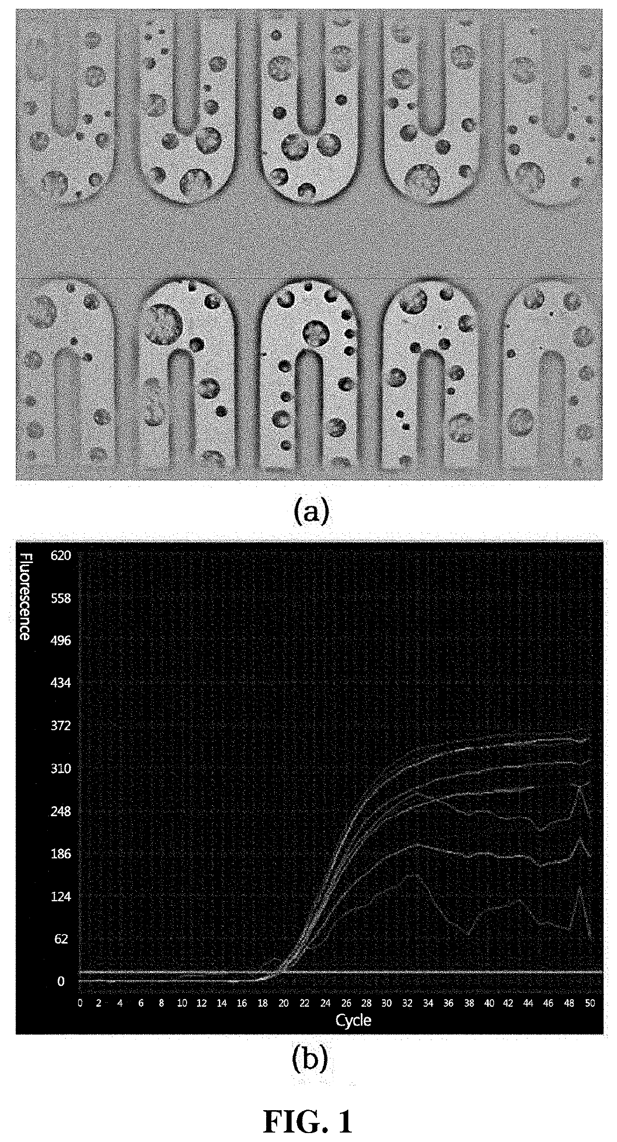
[0067]PCR was carried out using a microfluidic chip having an inlet / outlet structure according to the present disclosure.

[0068]The MERS COV-SPIKE detection kit (nano-biosys) was used as the PCR sample, the microfluidic chip was applied to G2-4 (nano-biosys) which is a PCR apparatus, the sample was introduced into the inlet of the microfluid chip until being filled up to the upper end of the outlet, and thereafter, DW8419 (DawonSchem) was poured as a sealing material so that the sealing material was filled from the fluid inlet part and finally filled up to the fluid outflow part.

[0069]The sealing material was irradiated with ultraviolet ray having a peak wavelength of 360 nm at about 600 mJ / cm2 for about 5 seconds to complete the sealing of the microfluidic chip.

[0070]The defective rate test, the internal bubble test of the fluid chip and the PCR performance test were performed for the sealed PCR chip. The test was perf...


PUM


Abstract

Provided is a microfluidic chip having an inlet / outlet structure optimized for sealing an inlet / outlet of a microfluidic chip using a UV curable sealing material, a microfluidic chip having the inlet / outlet structure, and a method of sealing the inlet / outlet of the microfluidic chip using a UV curable sealing material. It is possible to provide a semi-permanent seal with less contamination from a fluid sample or a harmful reagent, and the inlet / outlet of the microfluidic chip can be firmly sealed using simple equipment and without high-temperature / high-pressure conditions. By using the inlet / outlet structure of the microfluidic chip and the sealing method thereof, it is possible not only to improve the accuracy and deviation of the reaction result as the generation of bubbles is suppressed even when a predetermined reaction is performed on the microfluidic chip, but also it is possible to apply a fully automated system by eliminating the need for ancillary equipment such as a chip case and minimizing or eliminating manual operations.

Description

TECHNICAL FIELD[0001]The present disclosure provides an inlet / outlet structure of a microfluidic chip, a microfluidic chip having the inlet / outlet structure, and a method of sealing an inlet / outlet of the microfluidic chip. In particular, the present disclosure is related to an inlet / outlet structure of a microfluidic chip that is optimized for sealing the inlet / outlet of a microfluidic chip using a UV curable sealant, a microfluidic chip having the inlet / outlet structure, and a method of sealing the inlet / outlet of the microfluidic chip using the UV curable sealant.BACKGROUND ART[0002]A microfluidic chip has a function of simultaneously performing various experimental conditions by flowing fluid through a microfluidic channel. In particular, a microchannel is made using a substrate (or a chip material) such as plastic, glass, silicon, etc., and a fluid (e.g., a liquid sample) is moved through such a channel. Thereafter, it may be mixed and reacted in a plurality of chambers in a mi...

Claims


Application Information

Patent Timeline
Patent Type & Authority Patents(United States)
IPC IPC(8): B01L3/00B01L7/00
CPCB01L3/565B01L3/502707B01L3/502715B01L7/525B01L7/52B01L2200/0684B01L2200/0689B01L2300/08G01N35/08B01L2200/141B01L2300/041B01L2300/12B01L2200/10
Inventor KIM, SUNG WOOJEONG, SEUNG MINBYUN, JAE YOUNG
Owner NANOBIOSYS
Why Eureka
Try Eureka