
Solid-state image sensor and method of manufacturing the same

a solid-state image sensor and image sensor technology, applied in the field can solve the problems of insufficient resolution performance, adversely affecting the characteristics of solid-state image sensors, and insufficient resolution performan

Active Publication Date: 2021-12-21
TOPPAN PRINTING CO LTD
View PDF26 Cites 0 Cited by
  • Summary
  • Abstract
  • Description
  • Claims
  • Application Information

AI Technical Summary

Benefits of technology

The patent text explains that when color filters are made thinner and the concentration of pigments in the material increased to achieve desired spectral characteristics, the amount of photocurable component in the material is reduced, which can result in insufficient photocuring of the color filter layer. This can lead to shape deterioration, non-uniformity, and deformation in the color filter layer. Increasing the exposure amount during curing to ensure sufficient photocuring can also cause a problem of reducing throughput.

Problems solved by technology

In this case, however, light leaking from a color filter may enter an adjacent color filter, which leads to formation of a microlens having an appropriate size and shape.
However, a problem has occurred in which the small pixel size leads to insufficient resolution performance of the color filter layer formed by patterning by a photolithography process and this adversely affects characteristics of the solid-state image sensor.
In a solid-state image sensor having a pixel size of 1.4 μm or less or of close to 1.1 μm or 0.9 μm on each side, insufficient resolution performance results in color unevenness caused by a pattern shape defect.
When such a color filter layer is formed by patterning by a photolithography process, a portion (an ineffective portion of a pixel) originally to be removed is not completely removed and remains as a residue, and adversely affects pixels of other colors.
At this time, a problem has occurred in which when measures such as extension of development time are taken to remove the residue, cured necessary pixels are also peeled off.
When the color filters have a large thickness, however, smaller pixels tend to cause lower resolution such as rounded corners of the color filters formed by patterning.
When the pigment concentration is high, however, in some cases, light necessary for a photocuring reaction does not reach a bottom of a color filter layer, and this may lead to insufficient curing of the color filter layer.
This causes a problem in which the color filter layer is peeled off at a development step during photolithography, so that pixel defects occur.
This leads to insufficient photocuring of the color filter layer.
Furthermore, when an exposure amount during curing is increased to obtain sufficient photocuring, a problem of reduction in throughput occurs.
Due to a higher-definition pattern of a color filter layer, a thickness of the color filter layer not only causes a problem in the manufacturing process but also influences the characteristics of the solid-state image sensor.
In this case, a color mixture problem occurs.
The color mixture problem becomes apparent as a pixel size becomes smaller and an aspect ratio between the pixel size defining a pattern size and the thickness of the color filter becomes larger.
Furthermore, a problem regarding color mixture of incident light also becomes apparent when due to a material of a flattening layer and the like formed on a substrate in which photoelectric conversion elements are provided, a distance between a color filter pattern and the photoelectric conversion elements becomes long.
In this case, a ratio of a pigment component contained in the color filter material is increased, and thus the color filter material contains an insufficient amount of photosensitive component.
This has caused problems in which no resolution performance is obtained, a residue is more likely to remain, and pixels are more likely to be peeled off.
Thus, characteristics of the solid-state image sensor become deteriorated.

Method used


Image

  • Solid-state image sensor and method of manufacturing the same
  • Solid-state image sensor and method of manufacturing the same
  • Solid-state image sensor and method of manufacturing the same

Examples


second embodiment

[0160]A solid-state image sensor and a method of manufacturing the solid-state image sensor according to a second embodiment of the present invention will be described below with reference to FIGS. 10(a)-10(d). The solid-state image sensor according to the second embodiment of the present invention has a structure similar to that of the first embodiment.

[0161]The second embodiment differs from the first embodiment in a step during curing of the first-color color filter. Thus, a step of curing the first-color color filter will be described.

[0162]The solid-state image sensor according to the present embodiment is characterized in that the first-color color filter material contains no photosensitive resin material and is composed of only a thermosetting resin. Since the first-color color filter material contains only the thermosetting resin, the solid-state image sensor according to the present embodiment has an advantage that the pigment concentration can be increased and thus the fir...

third embodiment

[0171]A solid-state image sensor and a method of manufacturing the solid-state image sensor according to a third embodiment of the present invention will be described below with reference to FIGS. 11(a)-11(d).

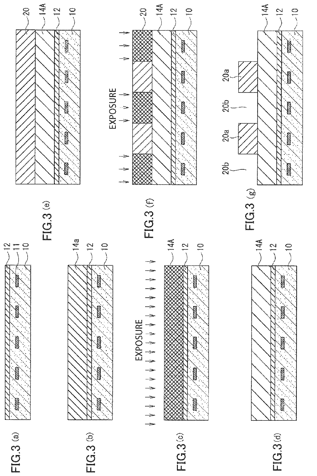
[0172]The solid-state image sensor according to the present embodiment is characterized in that the first-color color filter material contains only a photosensitive resin as a curable component. The configuration containing a photosensitive resin material is similar to that of the color filter forming step by photolithography using a photosensitive color resist of a conventional method. In the present embodiment, however, the photosensitive resin is used, but conventional patterning is not performed. Instead, photocuring by entire surface exposure is performed, followed by heat curing to evaporate water from the color filter by high temperature heating. Accordingly, as compared with the conventional method, the present embodiment can reduce the amount of photosensitive curable ...

fourth embodiment

Modified Examples of Fourth Embodiment

[0227](1) In the method of manufacturing the solid-state image sensor according to the fourth embodiment, the solid-state image sensor may be manufactured by employing a step of curing the first-color color filter similar to that of the second embodiment (see FIGS. 10(a)-10(d)). Effects and the like are similar to those of the third embodiment.

[0228](2) In the method of manufacturing the solid-state image sensor according to the fourth embodiment, the method of manufacturing the solid-state image sensor according to the third embodiment (see FIGS. 11 and 12) may be employed.

[0229]The solid-state image sensor is characterized in that the first-color color filter material contains only a photosensitive resin as a curable component. The configuration containing a photosensitive resin material is similar to that of the color filter forming step by photolithography using a photosensitive color resist of a conventional method. In the present embodimen...


PUM

PropertyMeasurementUnit
temperatureaaaaaaaaaa
pixel sizeaaaaaaaaaa

Abstract

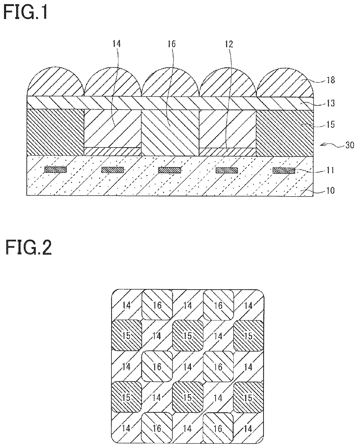
A solid-state image sensor including a semiconductor substrate having photoelectric conversion elements being two-dimensionally formed therein, and a color filter layer formed on the semiconductor substrate and having color filters of colors being two-dimensionally formed therein in a pattern such that the color filters correspond respectively to the photoelectric conversion elements. The color filter layer satisfies formulas (1) and (2):200≤A≤700  (1)C≤A+200  (2)where A represents a thickness in nm of a first-color color filter of a first color among the colors, and C represents a thickness in nm of color filters of colors other than the first color.

Description

CROSS-REFERENCE TO RELATED APPLICATIONS[0001]The present application is a continuation of International Application No. PCT / JP2017 / 046173, filed Dec. 22, 2017, which is based upon and claims the benefits of priority to Japanese Application No. 2016-253556, filed Dec. 27, 2016, and Japanese Application No. 2016-253650, filed Dec. 27, 2016. The entire contents of all of the above applications are incorporated herein by reference.BACKGROUND OF THE INVENTIONField of the Invention[0002]The present invention is a technique related to a solid-state image sensor including photoelectric conversion elements such as a CCD or a CMOS sensor.Discussion of the Background[0003]In recent years, solid-state image sensors, such as a CCD (charge-coupled device) and a CMOS (complementary metal-oxide semiconductor) sensor, mounted in digital cameras and the like, have a higher number of pixels and a smaller size. Particularly small solid-state image sensors have a pixel size smaller than 1.4 μm×1.4 μm.[0...

Claims


Application Information

Patent Timeline
Patent Type & Authority Patents(United States)
IPC IPC(8): H01L27/146G02B5/20G02B3/00H04N23/12
CPCH01L27/14621G02B5/201H01L27/1464H01L27/14685G02B3/0056H01L27/14627G02B5/20H01L27/146H04N23/12
Inventor IMOTO, TOMOHIROTAKAHASHI, SATOSHI
Owner TOPPAN PRINTING CO LTD
Learn More