
Cache memory and method for controlling the same

a technology of cache memory and memory access, applied in the field of cache memory, can solve the problems of data reusability low, slow memory access speed, bottleneck of processor performance, etc., and achieve the effect of high reusability, high reusability and high reusability

Active Publication Date: 2022-01-04
MITSUBISHI ELECTRIC CORP
View PDF6 Cites 0 Cited by
  • Summary
  • Abstract
  • Description
  • Claims
  • Application Information

AI Technical Summary

Benefits of technology

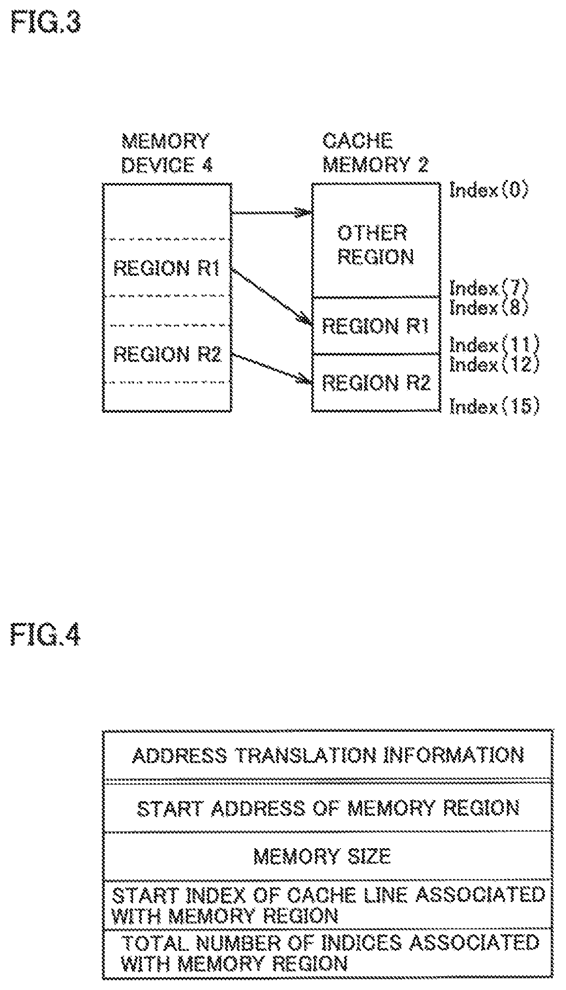
The patent text describes a way to organize memory to improve performance. By separating memory regions that store data that is frequently used, the system can also separate cache lines that are used for that data. This results in faster processing times because cache lines storing frequently used data are not replaced with data that is less frequently used.

Problems solved by technology

The processing speed for memory access is slower than the operating speed of a processor, and the delay time in memory access is thus a bottleneck for the performance of the processor.
By the way, in applications for scientific computing and image processing, etc., data is sequentially processed and data reusability is thus low.
Thus, if the access frequency of data having low reusability is higher than the access frequency of data having high reusability, a cache line storing the data having high reusability may end up being replaced with data that has low reusability.

Method used


Image

  • Cache memory and method for controlling the same
  • Cache memory and method for controlling the same
  • Cache memory and method for controlling the same

Examples


embodiment 1

[0039][One Example of Information Processing Apparatus]

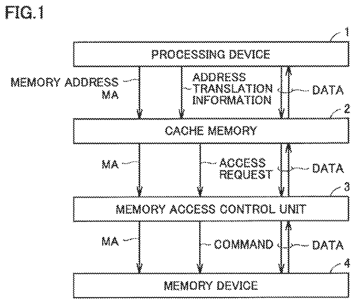
[0040]FIG. 1 is a block diagram showing one example configuration of an information processing apparatus in which a cache memory according to Embodiment 1 is implemented. The configuration of the information processing apparatus of FIG. 1 is also applicable to Embodiments 2 and 3. Referring to FIG. 1, the information processing apparatus includes a processing device 1, a cache memory 2, a memory access control unit 3, and a memory device 4.

[0041]Processing device 1 may be a part of a processor for executing programmed instructions, or a circuit that is built using an ASIC (Application Specific Integrated Circuit) or a FPGA (Field Programmable Gate Array).

[0042]Memory device 4 holds data for processing by processing device 1. Memory device 4 corresponds to a main memory of a microcomputer. Memory device 4 is configured of a general-purpose DRAM (Dynamic Random Access Memory), for example.

[0043]Cache memory 2 is a high-speed memor...

embodiment 2

[0105]Embodiment 2 will be described with reference to the mapping scheme of the cache memory being the direct mapping.

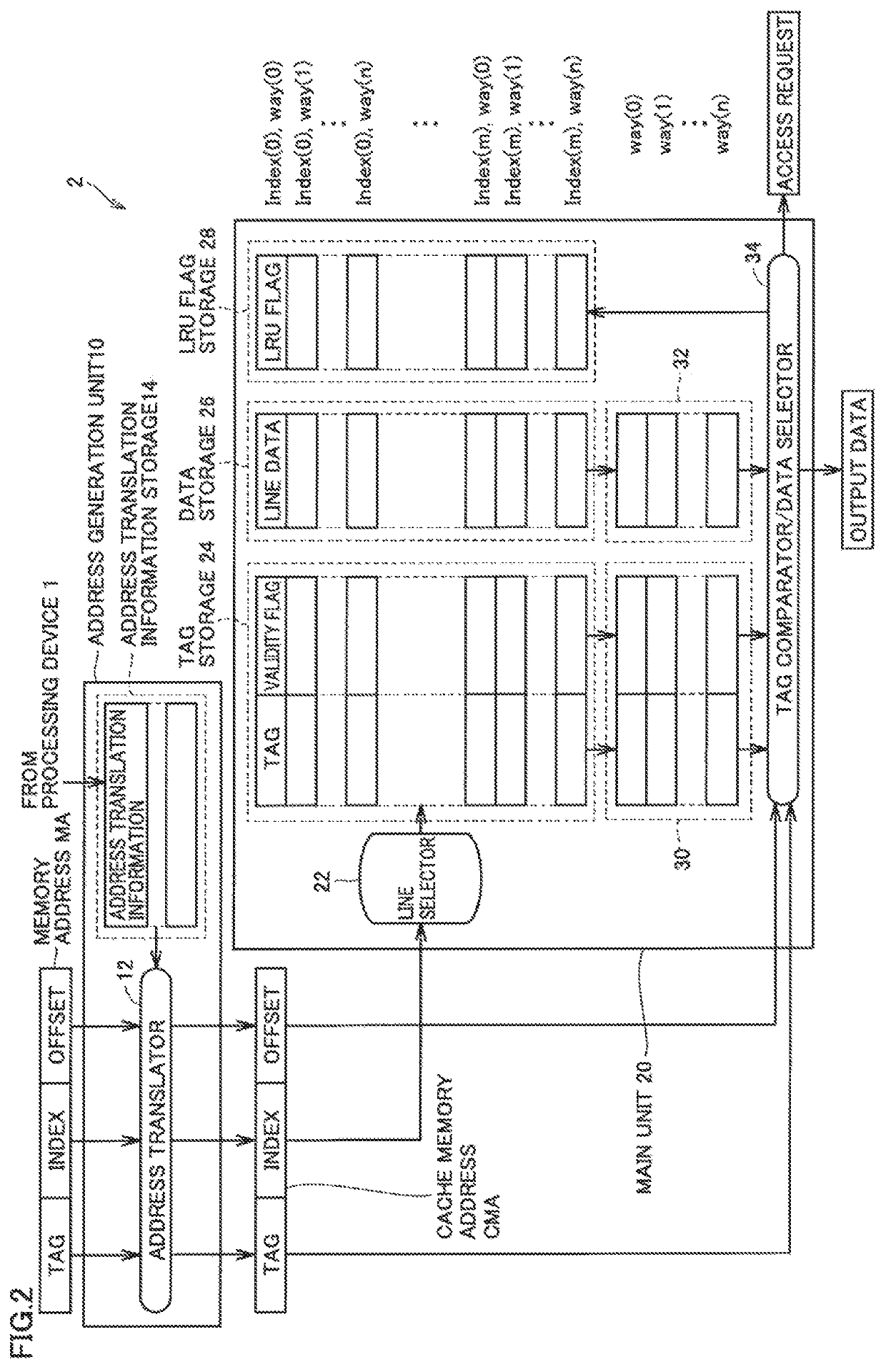
[0106]FIG. 9 is a block diagram showing one example configuration of a cache memory according to Embodiment 2. Cache memory 2A of FIG. 9 is different from cache memory 2 of FIG. 2 with respect to the configuration of main unit 20A. Specifically, cache lines in main unit 20A are not provided with ways associated with respective indices, and, additionally, main unit 20A does not include LRU flag storage 28. The rest of configuration of cache memory 2A of FIG. 9 is the same as cache memory 2 of FIG. 2. Thus, like reference signs refer to like or corresponding parts and the description thereof will not be repeated.

[0107]FIG. 10 is a flowchart showing an operation of the cache memory of FIG. 9. In the flowchart of FIG. 9, like reference signs refer to steps like or corresponding to those shown in the flowchart according to Embodiment 1, and the description thereof will n...

embodiment 3

[0115][Schematic Configuration of Cache Memory]

[0116]Embodiment 3 will be described with reference to the mapping scheme of a cache memory being fully associative mapping. FIG. 11 is a block diagram showing one example configuration of a cache memory according to Embodiment 3.

[0117]Referring to FIG. 11, in the case of the fully associative mapping, input memory address MA includes a tag in upper bits and an offset in lower bits, and is not provided with an index. Cache memory address CMA translated from input memory address MA by address translator 12 includes additional information corresponding to an index which is added between the tag and the offset. The additional information does not specify one index, but specifies a range of indices (the upper limit and the lower limit). Data and the tag can be stored in any cache line within this index range. This can limit the range of cache lines, according to a memory region to be accessed which is associated with memory address MA, ther...


PUM


Abstract

In a cache memory, a main unit stores memory address information which is associated with part of data stored in a memory space to be accessed, on a cache line-by-cache line basis. The memory space is divided into a plurality of memory regions. The address generation unit generates a cache memory address from a memory address specified by an external access request, based on a memory region among the plurality of memory regions which is associated with the memory address specified by the access request. A main unit is searched according to the cache memory address, thereby searching and replacing different ranges of cache lines for different memory regions.

Description

TECHNICAL FIELD[0001]The present disclosure relates to a cache memory and a method for controlling the same.BACKGROUND ART[0002]The processing speed for memory access is slower than the operating speed of a processor, and the delay time in memory access is thus a bottleneck for the performance of the processor. In order to hide the delay time in memory access, a small-capacity, high-speed memory, called a cache memory, is used which stores data having high reusability.[0003]Cache memory stores data per unit called a line. Mapping schemes for associating a memory address and a line in a cache memory are classified into direct mapping, set-associative mapping, fully associative mapping, etc.[0004]On a cache miss, data stored in a cache line is replaced with data in a memory device. As a method for this replacement, an algorithm referred to as LRU (Least Recently Used) is generally used. The LRU is a method in which data stored in the least recently used line is first replaced with dat...

Claims


Application Information

Patent Timeline
Patent Type & Authority Patents(United States)
IPC IPC(8): G06F12/06G06F12/10
CPCG06F12/0646G06F12/10G06F2212/1041G06F12/0895G06F12/0873
Inventor YAMAGUCHI, KEITA
Owner MITSUBISHI ELECTRIC CORP
Learn More