Inverted microstrip travelling wave patch array antenna system

a patch array and microstrip technology, applied in the field of microstrip antenna systems, can solve the problems of difficult to meet the requirements of microstrip antennas, high fabrication and assembly costs, and complicated manufacturing of microstrip antennas

Active Publication Date: 2022-01-11
GM GLOBAL TECH OPERATIONS LLC
View PDF13 Cites 0 Cited by
  • Summary
  • Abstract
  • Description
  • Claims
  • Application Information

AI Technical Summary

Benefits of technology

[0003]Microstrip or patch antennas have been used in relatively low gain applications of short-range wireless systems. A microstrip antenna usually consists of a conductive patch on a grounded dielectric substrate. The bandwidth of a typical microstrip antenna tends to be narrow. In addition, microstrip antennas typically use vias. A via (vertical interconnect access) is an electrical connection between layers in an electronic circuit that pass through one or more adjacent layers. When these layers are digital circuit boards operating with radio frequency or microwave signals they have high noise sensitivity and tight impedance tolerances than traditional digital circuit boards. The use of vias penetrating such boards makes achieving those requirements challenging. As a result, microstrip antennas are complicated to manufacture and have relatively high fabrication and assembly costs.

Problems solved by technology

The use of vias penetrating such boards makes achieving those requirements challenging.
As a result, microstrip antennas are complicated to manufacture and have relatively high fabrication and assembly costs.

Method used


Image

  • Inverted microstrip travelling wave patch array antenna system
  • Inverted microstrip travelling wave patch array antenna system
  • Inverted microstrip travelling wave patch array antenna system

Examples


Embodiment Construction

[0034]The following detailed description is merely exemplary in nature and is not intended to limit the application and uses. Furthermore, there is no intention to be bound by any expressed or implied theory presented in the preceding technical field, background, brief summary or the following detailed description. As used herein, the term module refers to an application specific integrated circuit (ASIC), an electronic circuit, a processor (shared, dedicated, or group) and memory that executes one or more software or firmware programs, a combinational logic circuit, and / or other suitable components that provide the described functionality.

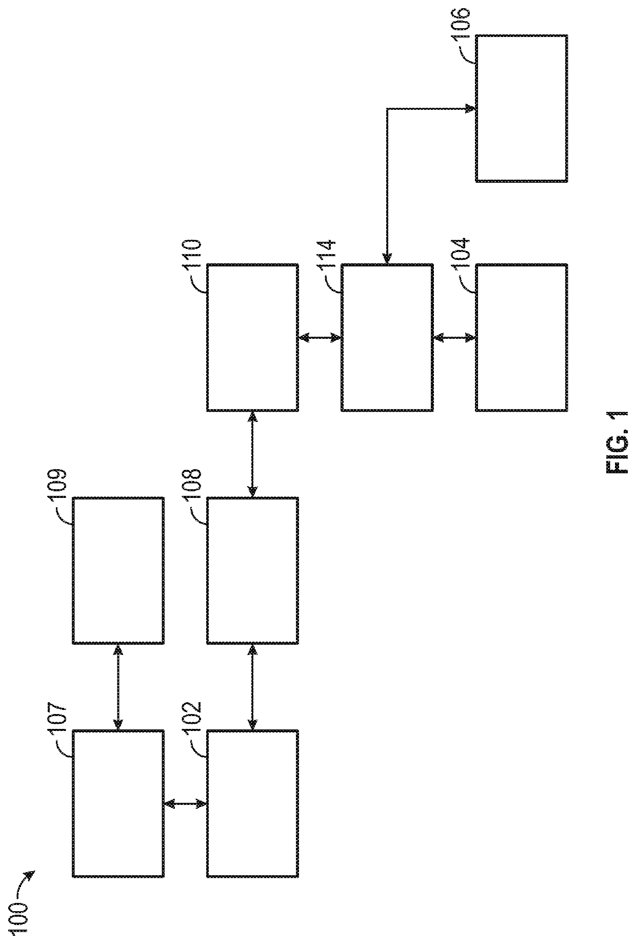
[0035]This description discloses configurations and implementations of antenna systems for operating at high frequencies, such as 235 GHz, a sub-terahertz frequency range for uses such as radar imaging. Embodiments of antenna architectures and components disclosed herein in general, may use a thin interposer substrate of a dielectric material such...


PUM


Abstract

An antenna system includes a substrate of a dielectric material. A conductive feed joins a number of conductive patches arranged in a line forming an array. The conductive patches are spaced from one another and the array is disposed on the substrate. The array has first and second sides. A first ground plane is disposed on the first side of the array and is spaced apart from the array. A number of conducting pillars ground the substrate to the first ground plane, and the conducting pillars define a second ground plane on the substrate. The array is configured to radiate a radiation pattern characterized by a first beam width in a first plane and a second beam width in a second plane perpendicular to the first plane, wherein the first beam width is wider than the second beam width.

Description

INTRODUCTION[0001]The technical field generally relates to antennas, and more particularly relates to microstrip antenna systems that support precise location determinations for applications such as radar imaging.[0002]In general, range, velocity, azimuth angle and other target attributions are measured by radar devices. In some applications, such as radar systems for automobiles, it may be desirable to provide information representing or relating to the characteristics of a target or object detected by the radar system. This information may be used to evaluate the detected target or object. Typical automotive imaging radar sensors operate at conventional frequencies of 76-81 GHz. In applications such as object detection and classification, fast and precise capabilities are desirable for immediate determinations regarding approaching objects. The azimuth and the elevation of an object are typical parameters of interest. Receiving object information requires an antenna that supports ...

Claims


Application Information

Patent Timeline
Patent Type & Authority Patents(United States)
IPC IPC(8): H01Q1/32H01Q1/48H01Q21/00H01Q21/08H01Q1/52
CPCH01Q1/3233H01Q1/48H01Q1/523H01Q21/0068H01Q21/08H01Q1/50H01Q21/065H01Q13/206
Inventor KONA, KEERTI S.
Owner GM GLOBAL TECH OPERATIONS LLC
Why Eureka
Try Eureka