Thin film transistor substrate and method of fabricating same

a thin film transistor and substrate technology, applied in the field of thin film transistor substrates, can solve the problems of poor achieve the effects of reducing the influence of bias stress, preventing electron trapping, and improving the reliability of the thin film transistor substra

Active Publication Date: 2022-02-01
SHENZHEN CHINA STAR OPTOELECTRONICS SEMICON DISPLAY TECH CO LTD
View PDF6 Cites 0 Cited by
  • Summary
  • Abstract
  • Description
  • Claims
  • Application Information

AI Technical Summary

Benefits of technology

[0016]Beneficial effects of an embodiment of the present disclosure are that, a thin film transistor substrate and a method of fabricating the same are provided. The gate insulating layer adopts a two-layer structure, one layer is a silicon oxide layer, and another layer is a silicon nitride layer. The silicon oxide layer is formed on the active layer, and the silicon nitride layer is formed on the silicon oxide layer. Hydrogen ions in the silicon nitride layer diffuse into the active layer, hindering trapping of electrons by the defect state, reducing influence of a bias stress on characteristics of the thin film transistor substrate, and improving reliability of the thin film transistor substrate. In addition, silicon nitride has a high dielectric constant, which can improve field effect mobility of the thin film transistor substrate.

Problems solved by technology

Characteristics of the thin film transistor substrate are greatly affected, and this results in poor reliability of the thin film transistor substrate.

Method used


Image

  • Thin film transistor substrate and method of fabricating same
  • Thin film transistor substrate and method of fabricating same
  • Thin film transistor substrate and method of fabricating same

Examples


Embodiment Construction

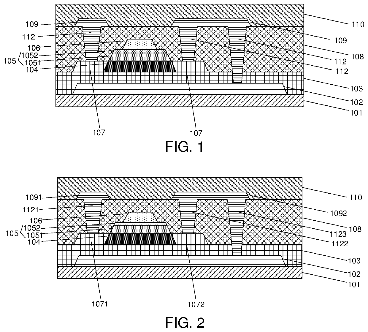
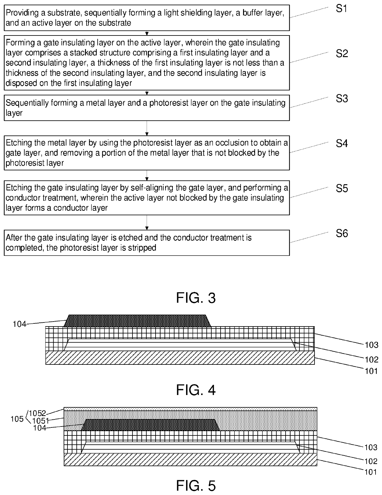
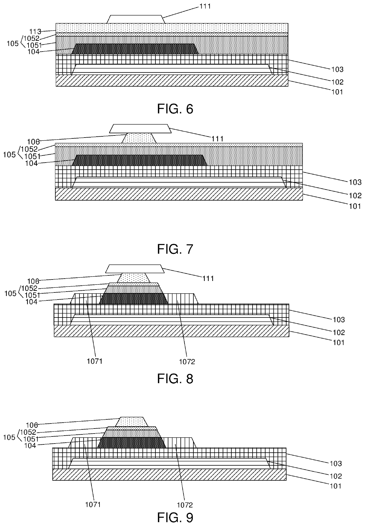
[0032]The technical solutions in the embodiments of the present invention are clearly and completely described in the following with reference to the accompanying drawings in the embodiments of the present invention. It is obvious that the described embodiments are only a part of the embodiments of the present invention, but not all embodiments. All other embodiments obtained by a person skilled in the art based on the embodiments of the present invention without creative efforts are within the scope of the present invention.

[0033]In the description of the present application, it is to be understood that the terms of the orientation or positional relationship of the indications terms “center”, “longitudinal”, “transverse”, “length”, “width”, “thickness”, “upper”, “lower”, “front”, “back”, “left”, “right”, “vertical”, “horizontal”, “top”, “bottom”, “inner”, “outer”, “clockwise”, “counterclockwise”, and the like are based on the orientation or positional relationship shown in the draw...


PUM

PropertyMeasurementUnit
thicknessaaaaaaaaaa
thicknessaaaaaaaaaa
thicknessaaaaaaaaaa

Abstract

A thin film transistor substrate and a method of fabricating same are provided.The thin film transistor substrate includes a substrate, a light shielding layer disposed on the substrate, a buffer layer disposed on the light shielding layer, an active layer disposed on the buffer layer, and a gate insulating layer disposed on the active layer. The gate insulating layer includes a stacked structure including a first insulating layer and a second insulating layer.

Description

CROSS-REFERENCE TO RELATED APPLICATIONS[0001]This is the U.S. National Stage of International Patent Application No. P PCT / CN2019 / 113014, filed Oct. 24, 2019, which in turn claims the benefit of Chinese Patent Application No. 201910654433.1, filed Jul. 19, 2019.FIELD OF INVENTION[0002]The present disclosure relates to the field of display panel technologies, and more particularly to a thin film transistor substrate and a method of fabricating the same.BACKGROUND OF INVENTION[0003]In the field of display technologies, flat panel display devices such as liquid crystal displays (LCDs) and organic light emitting diode (OLED) displays have gradually replaced cathode display screens, are widely used in mobile phones, televisions, personal digital assistants, digital cameras, notebook computers, desktop computers, and other consumer electronic products, and have become the mainstream in display devices.[0004]Generally, a liquid crystal display panel includes a color filter (CF) substrate, ...

Claims


Application Information

Patent Timeline
Patent Type & Authority Patents(United States)
IPC IPC(8): H01L29/417H01L29/786H01L29/66H01L29/40
CPCH01L29/41733H01L29/401H01L29/66969H01L29/786H01L29/78681H01L29/78606H01L29/78633H01L29/42384H01L29/7869
Inventor MA, QIANZHOU, XINGYU
Owner SHENZHEN CHINA STAR OPTOELECTRONICS SEMICON DISPLAY TECH CO LTD
Why Eureka
Try Eureka