Stack structure and touch sensor
a stack structure and touch sensor technology, applied in the field of stack structures, can solve the problems of increasing the size of silver nanowires, delaying the yield rate of stack structures in etching processes, and increasing the wire diameter of silver nanowires, so as to reduce the difficulty of silver nanowire etching, and increase the process window and yield rate
- Summary
- Abstract
- Description
- Claims
- Application Information
AI Technical Summary
Benefits of technology
Problems solved by technology
Method used
Image
Examples
first embodiment
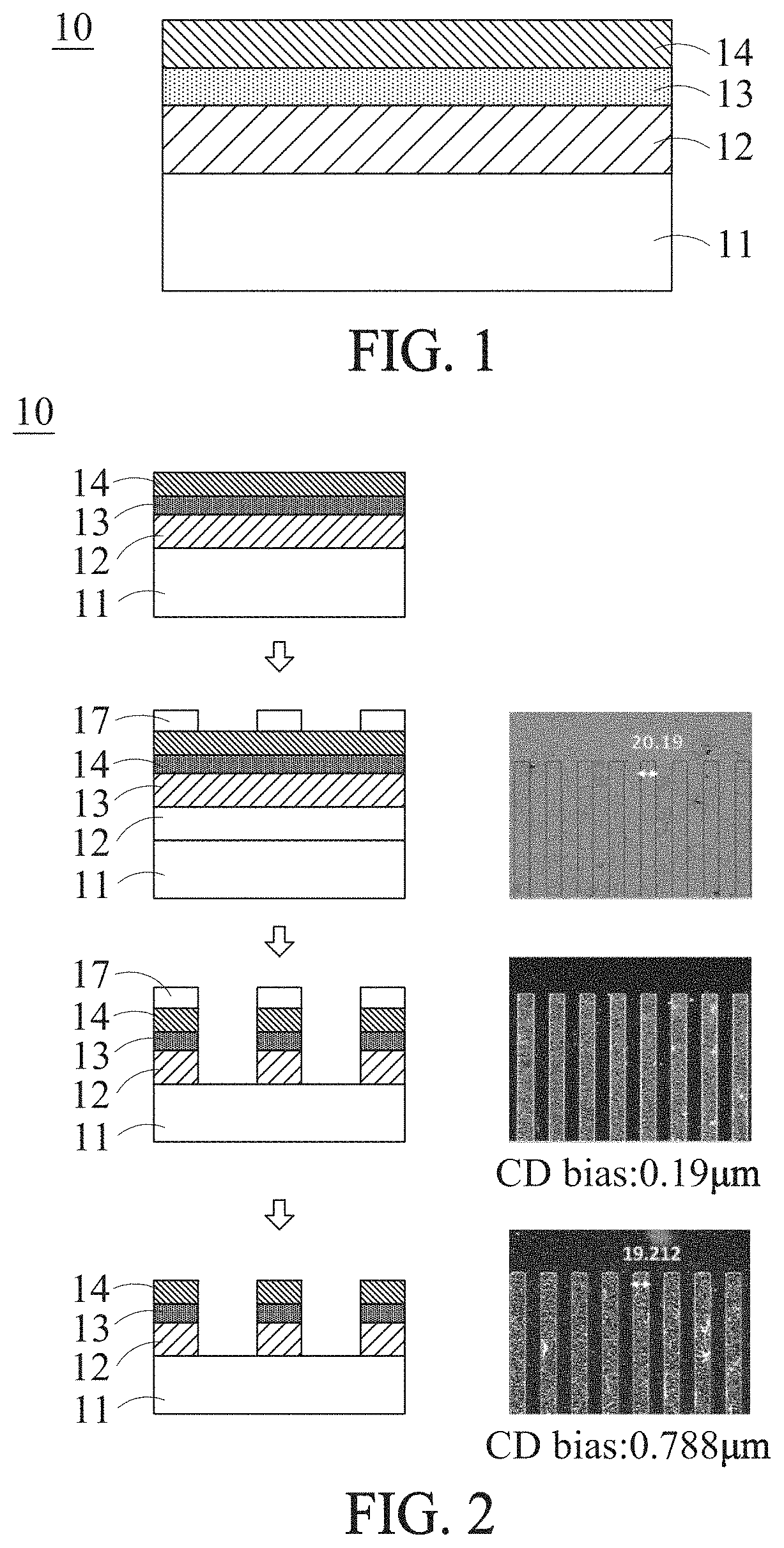
[0028]FIG. 1 is a schematic view of a stack structure 10 according to the first embodiment of the present disclosure. Referring to FIG. 1, the stack structure 10 in the first embodiment of the present disclosure comprises: a substrate 11, a copper layer 12 disposed on the substrate 11, a migration-proof layer 13 disposed on the copper layer 12, and a silver-nanowire layer 14 disposed on the migration-proof layer 13, wherein the migration-proof layer 13 is made of materials between copper and silver in galvanic series.
[0029]In this embodiment, the substrate 11 is a thin-film substrate, but the present disclosure is not limited thereto, and thus persons skilled in the art can select any other substrate as needed, such as polyethylene terephthalate (PET), cyclic olefin copolymer (COP), or colorless polyimide (CPI). For example, the substrate 11 may be a polymeric transparent plastic substrate with a thickness of 10 μm−150 μm.
[0030]In this embodiment, the copper layer 12 is made of pure...
second embodiment
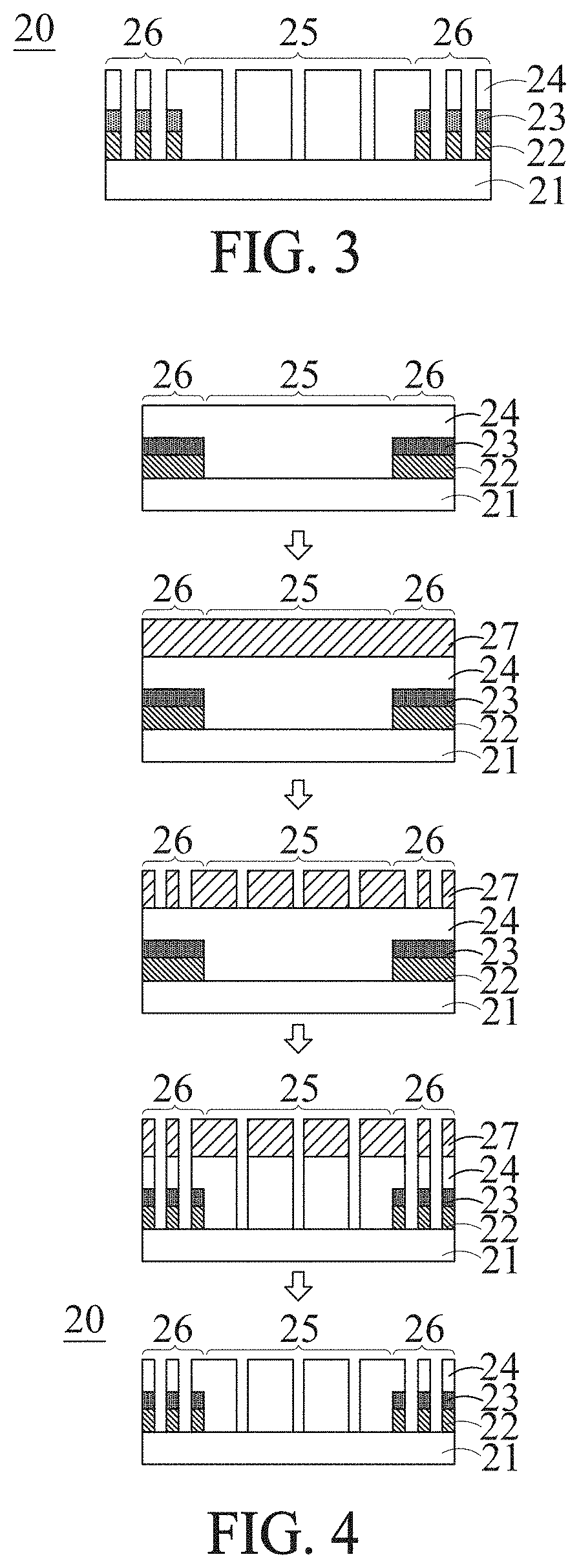
[0039]FIG. 3 is a schematic view of a touch sensor 20 according to the second embodiment of the present disclosure. Referring to FIG. 3, the touch sensor 20 comprises: a substrate 21, a copper layer 22 disposed on the substrate 21, a migration-proof layer 23 disposed on the copper layer 22, and a silver-nanowire layer 24 disposed on the migration-proof layer 23, wherein the migration-proof layer 23 is made of materials between copper and silver in galvanic series.
[0040]Referring to FIG. 3, the copper layer 22, the migration-proof layer 23, and the silver-nanowire layer 24 are patterned.
[0041]Referring to FIG. 3, in the touch sensor 20 of the second embodiment, the copper layer 22 and the migration-proof layer 23 are disposed on the edge of the substrate 21, defining a visible region 25 wherein the substrate 21 is not covered by the copper layer 22 and the migration-proof layer 23 and a peripheral wiring region 26 wherein the substrate 21 is covered by the copper layer 22 and the mig...
PUM
| Property | Measurement | Unit |
|---|---|---|
| critical dimension bias | aaaaa | aaaaa |
| stack structure | aaaaa | aaaaa |
| size | aaaaa | aaaaa |
Abstract
Description
Claims
Application Information


