Field-effect transistor without punch-through stopper and fabrication method thereof

a field-effect transistor and punch-through stopper technology, applied in the field of field-effect transistors, can solve the problems of degrading the performance and reliability of the cells of the field-effect transistor, affecting the overall process, and increasing power consumption, so as to achieve high productivity and yield, reduce the effect of reliability degradation

Active Publication Date: 2022-07-12
POSTECH ACAD IND FOUND
View PDF19 Cites 0 Cited by
  • Summary
  • Abstract
  • Description
  • Claims
  • Application Information

AI Technical Summary

Benefits of technology

[0019]Since the field effect transistor according to the present invention does not include a punch-through stopper, problems such as performance deterioration, reliability degradation, and variability of the device, which are attributable to formation of the punch-through stopper, are prevented.
[0020]In addition, since punch-through stoppers are not performed, the overall process can be simplified. That is, a difficult process (punch-through stopper) is eliminated from a manufacturing method of a field effect transistor, high productivity and yield can be achieved.

Problems solved by technology

However, as the cell size is reduced to tens of nanometers, the source-to-drain leakage current flowing into the region below the channel, which cannot be controlled via the gate, is increased, leading to increased power consumption.
However, even with the FinFET and the GAA FET, the problem cannot be effectively solved.
Therefore, interface states such as dangling bonds appear on the surface underneath the channel during STI deposition and thermal annealing processes, thereby degrading the performance and reliability of the cells of a field effect transistor.
Therefore, the step of forming punch-through stoppers is the most difficult to process during manufacturing of a conventional field effect transistor.
Therefore, it often results in process-related troubles and productivity and yield reduction problems.
Since the SEG involves a thermal process, there is a problem in that the impurities in the punch-through stopper formed through the punch-through stopper process diffuse into the channel, which lowers carrier mobility in the fabricated device.
As a result, device reliability and variability problems arise.

Method used


Image

  • Field-effect transistor without punch-through stopper and fabrication method thereof
  • Field-effect transistor without punch-through stopper and fabrication method thereof
  • Field-effect transistor without punch-through stopper and fabrication method thereof

Examples


first embodiment

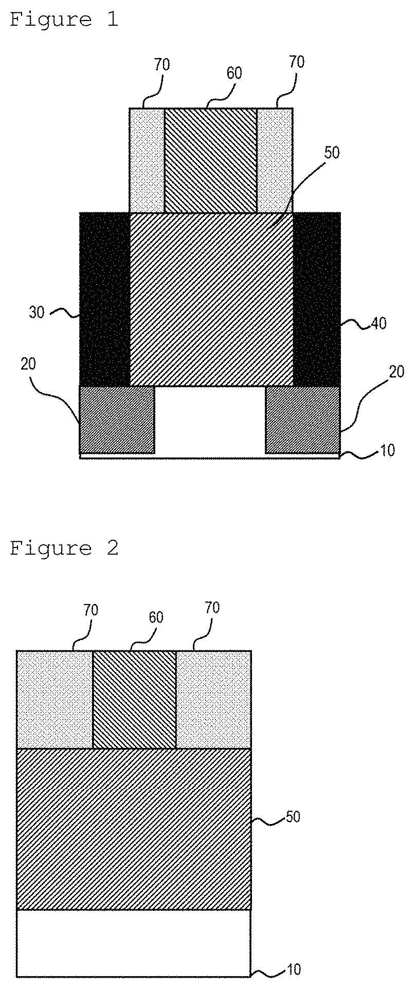
[0029]FIG. 1 is a cross-sectional view of a field effect transistor according to the present disclosure. Specifically, the field effect transistor basically has the same structure as a metal oxide semiconductor field effect transistor (MOSFET).

[0030]Referring to FIG. 1, the field effect transistor includes a substrate 10, a first insulating film 20, Source and drain regions 30 and 40, a channel 50, a gate 60, and a second insulating film 70.

[0031]A conventional field effect transistor has a structure in which a punch-through stopper is formed under the channel. However, in the structure of the field effect transistor according to the present invention, the first insulating film is formed in an upper portion of the substrate 10 to replace the punch-through stopper.

[0032]Specifically, the first insulating film 20 is embedded in the substrate 10, and the source and drain regions 30 and 40 are formed on the first insulating film 20. The first insulating film 20 is partially in contact w...

second embodiment

[0065]FIG. 8 is a cross-sectional view illustrating a nanosheet field effect transistor (NSFET), as one exemplary FET structure, according to the present invention. The structure of the NSFET shown in FIG. 8 is illustrated as a single stack in which nanosheets are stacked in three layers for convenience. However, the field effect transistor (FET) according to the present invention may have a multilayer single stack structure in which n or more layers are stacked. Alternatively, the field effect transistor may have a multilayer multi-stack structure including n or more stacks each stack being composed of n or more layers.

[0066]Referring to FIG. 8, the field effect transistor includes a substrate 110, first insulating films 120 partially embedded in an upper portion of the substrate 110, a source region 130 and a drain region 140 respectively positioned on the first insulating films 120, a plurality of horizontally extending channels 150 and a plurality of spacings 180 alternatively a...


PUM

PropertyMeasurementUnit
thicknessaaaaaaaaaa
thicknessaaaaaaaaaa
insulatingaaaaaaaaaa

Abstract

Disclosed is a field effect transistor including an insulating film disposed between a source / drain region and a substrate. Since the insulating film prevents current leakage under a channel, it is not necessary to form a punch-through stopper. Further disclosed is a method of forming a field effect transistor.

Description

CROSS REFERENCE TO RELATED APPLICATION[0001]The present application claims priority to Korean Patent Application No. 10-2019-0011571, filed on Jan. 30, 2019, the entire contents of which are incorporated herein for all purposes by this reference.DESCRIPTIONTechnical Field[0002]The present invention relates to a field effect transistor provided with an insulating film that prevents leakage current at the bottom of the channel and a method of manufacturing the same.Background Art[0003]A metal-oxide-semiconductor field effect transistor (MOSFET) is a device including three terminals respectively called a source, a drain, and a gate. The MOSFET has an N-type semiconductor channel or a P-type semiconductor channel. There are several types of MOSFETs. For example, MOSFETs can be classified into PMOSFETs and NMOSFETs according to a semiconductor material used therefor. There is also a CMOSFET in which both the PMOSFET and the NMOSFET are included.[0004]MOSFETs function as switches or ampli...

Claims


Application Information

Patent Timeline
Patent Type & Authority Patents(United States)
IPC IPC(8): H01L29/06H01L29/66H01L29/78
CPCH01L29/0653H01L29/6653H01L29/6681H01L29/66795H01L29/785H01L29/7853H01L29/78696H01L29/42392H01L29/66439H01L29/66545H01L29/66636H01L29/7848H01L29/0673H01L29/775B82Y10/00H01L29/7843H01L29/7849H01L29/06H01L29/517H01L29/0665H01L21/027H01L21/31105
Inventor BAEK, ROCK HYUNYOON, JUN SIKJEONG, JIN SULEE, SEUNG HWAN
Owner POSTECH ACAD IND FOUND
Why Eureka
Try Eureka