Superconductivity device comprising a phononic crystal

a phononic crystal and superconductivity technology, applied in the field of superconductivity, can solve the problems of increasing the overhead in cost and time, the decoherence and loss of co-pair superconductivity, and the increase of resistive losses, so as to suppress the normal conduction

Active Publication Date: 2022-08-23
NAT TECH & ENG SOLUTIONS OF SANDIA LLC
View PDF2 Cites 0 Cited by
  • Summary
  • Abstract
  • Description
  • Claims
  • Application Information

AI Technical Summary

Benefits of technology

[0007]According to the present invention, the superconducting transition width can be engineered by suppressing the phonon populations responsible for the Cooper-pair decoherence below the superconducting transition temperature (Tc) via phononic bandgap engineering. The invention is directed to a superconducting device comprising a two-dimensional phononic crystal (PnC) comprising a periodic array of holes or plugs in a superconducting matrix material, wherein the holes or plug material provide an acoustic impedance mismatch with the matrix material, wherein the matrix material has a superconducting transition temperature Tc, and wherein the phononic crystal has a phononic bandgap at a frequency that suppresses a decohering thermal phonon population just below the Cooper-frequency of the matrix material, thereby suppressing the normal conduction electron population near Tc and narrowing the width of the superconducting transition.

Problems solved by technology

As the temperature rises, approaching the transition temperature (Tc), interactions with thermal phonons result in Cooper-pair decoherence and loss of superconductivity.
In the neighborhood of Tc, resistive losses start increasing due to the increase in the thermal phonon noise and the subsequent disruption of the Cooper-pairs.
As such, almost all superconducting applications require cooling well below Tc to ensure a lossless system, which increases the required overhead in terms of cost and time.

Method used


Image

  • Superconductivity device comprising a phononic crystal
  • Superconductivity device comprising a phononic crystal
  • Superconductivity device comprising a phononic crystal

Examples


Embodiment Construction

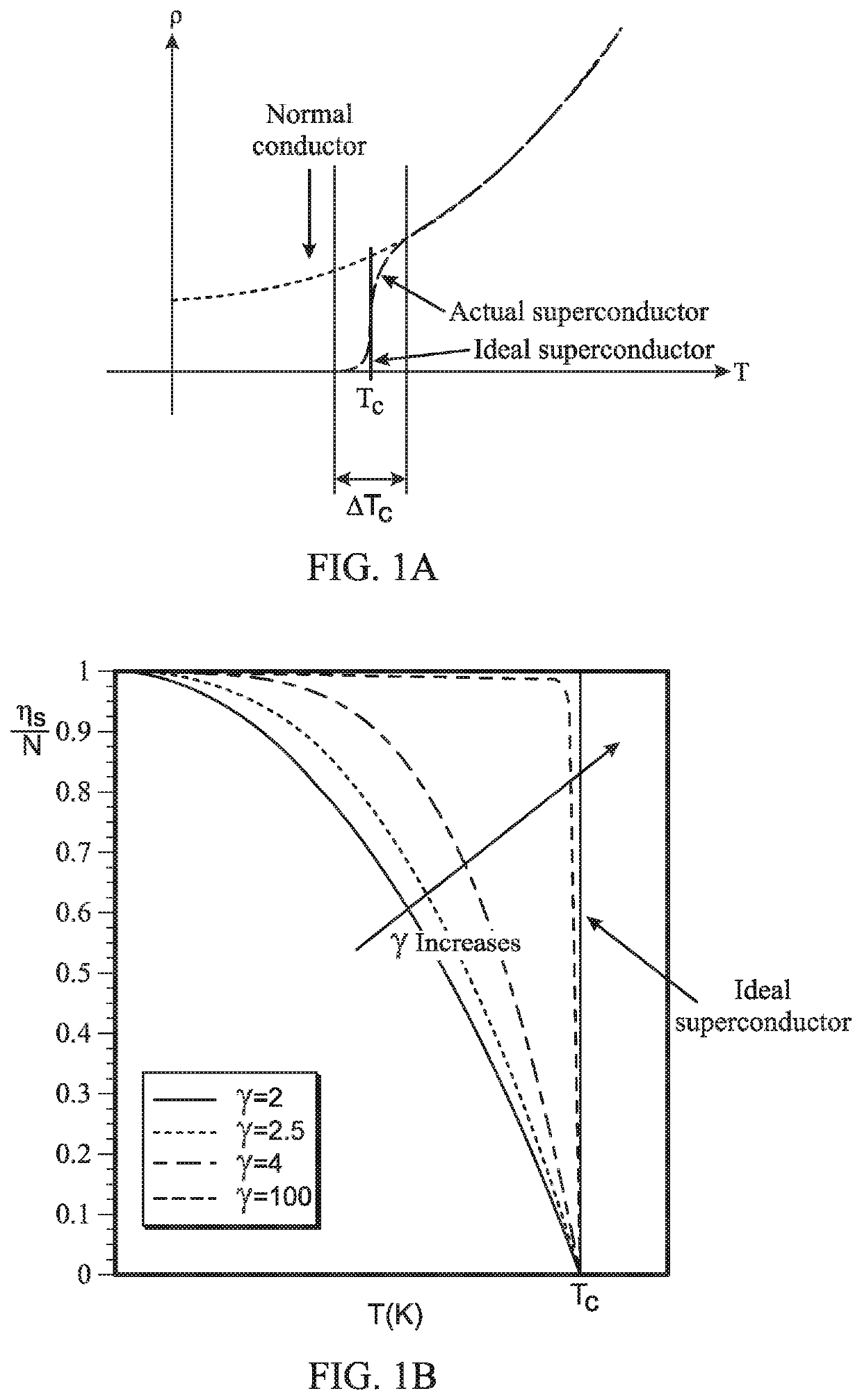
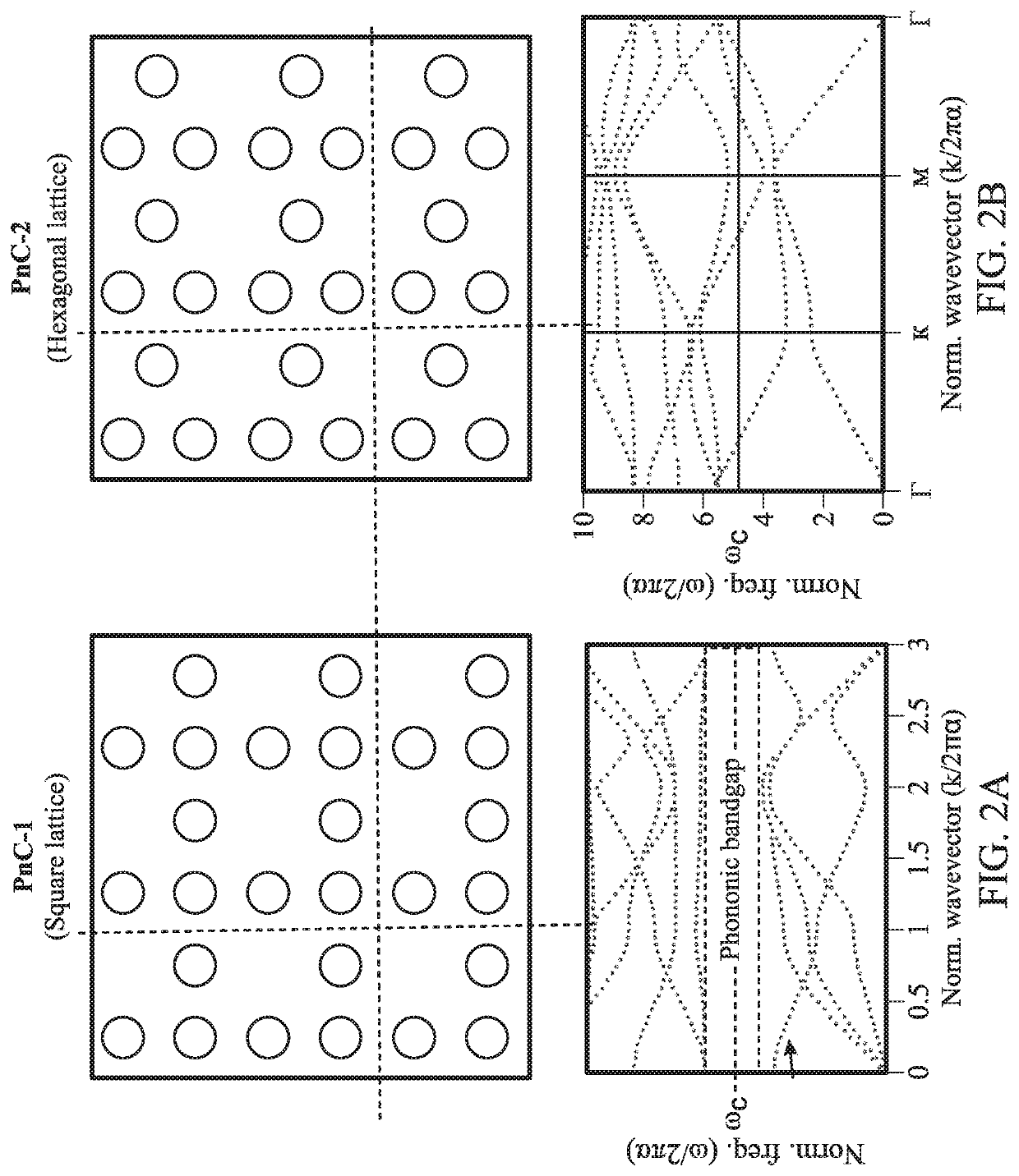
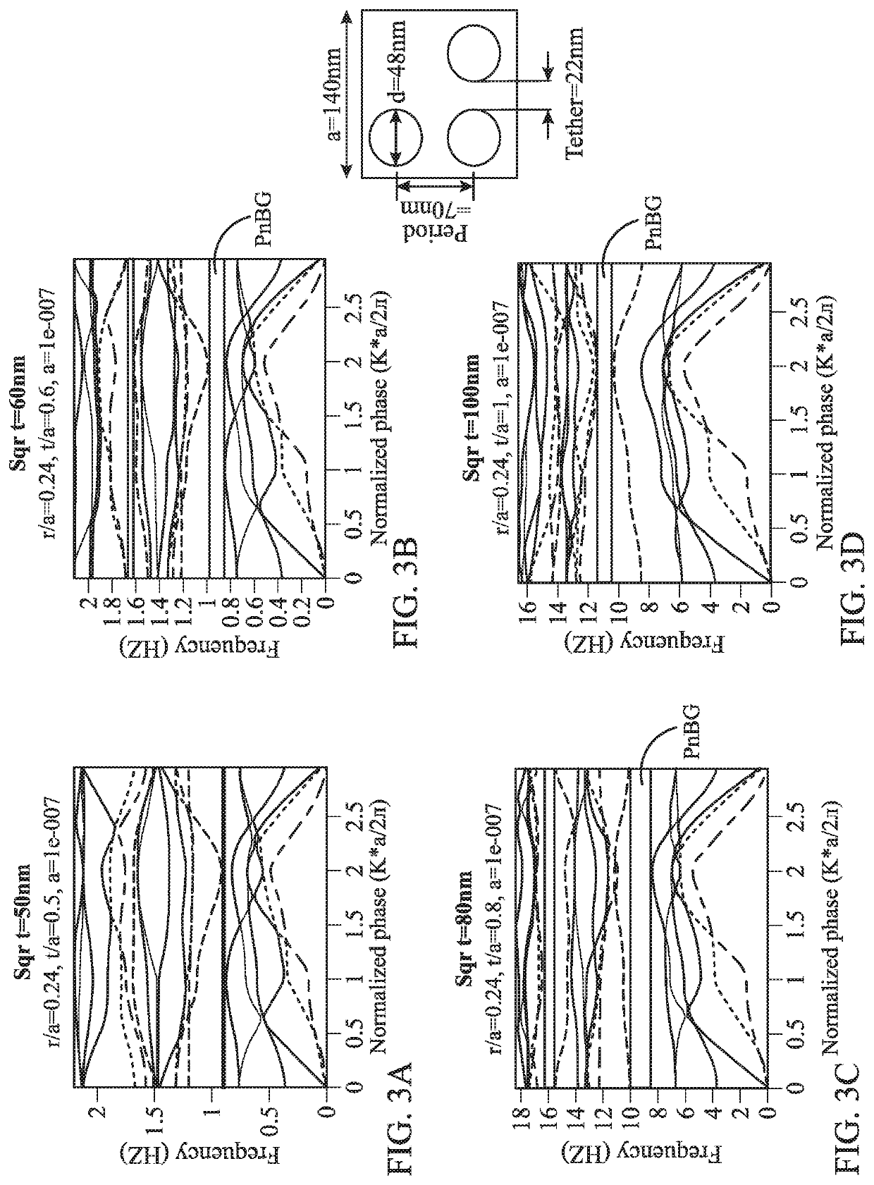
[0014]According to the present invention, the distribution of superconducting Cooper-pairs and unpaired normal-conducting electrons can be modified by selectively engineering which phonons can propagate in the superconductor. Changing the thermal background seen by the electrons can result in fewer quasi-particle excitations (i.e., normal electrons). Fundamentally, this phonon engineering route requires suppression of the phonon heat capacity of the superconductor near Tc. In particular, a phononic crystal (PnC) can be used to engineer a phononic frequency gap that suppresses the decohering thermal phonon population just below the Cooper-frequency (fc), and thus the normal conduction electron population. PnCs comprise periodic arrangements of phonon scattering centers embedded in a homogeneous background matrix with lattice spacing comparable to the acoustic wavelength. The scattering material has a density and / or elastic constant that is different than the matrix material. When pro...


PUM

PropertyMeasurementUnit
unit cell sizeaaaaaaaaaa
thicknessesaaaaaaaaaa
diameteraaaaaaaaaa

Abstract

The invention is directed to a device and method to engineer the superconducting transition width by suppressing the phonon populations responsible for the Cooper-pair decoherence below the superconducting transition temperature via phononic bandgap engineering. The device uses phononic crystals to engineer a phononic frequency gap that suppresses the decohering thermal phonon population just below the Cooper-frequency, and thus the normal conduction electron population. For example, such engineering can relax the cooling requirements for a variety of circuits yielding higher operational quality factors for superconducting electronics and interconnects.

Description

CROSS-REFERENCE TO RELATED APPLICATION[0001]This application claims the benefit of U.S. Provisional Application No. 62 / 639,362, filed Mar. 6, 2018, which is incorporated herein by reference.STATEMENT OF GOVERNMENT INTEREST[0002]This invention was made with Government support under Contract No. DE-NA0003525 awarded by the United States Department of Energy / National Nuclear Security Administration. The Government has certain rights in the invention.FIELD OF THE INVENTION[0003]The present invention relates to superconductivity and, in particular, to a superconducting device and a method to engineer superconductivity using a phononic crystal.BACKGROUND OF THE INVENTION[0004]According to BCS theory, superconductivity arises from the creation of Cooper-pairs, a coherent interaction of two opposite-spin electrons coupled by a lattice phonon. As the temperature rises, approaching the transition temperature (Tc), interactions with thermal phonons result in Cooper-pair decoherence and loss of...

Claims


Application Information

Patent Timeline
Patent Type & Authority Patents(United States)
IPC IPC(8): H01L39/12H01L39/22G06N10/00H01L39/16
CPCH01L39/12G06N10/00H01L39/16H01L39/223H10N60/85H10N60/12H10N60/30H10N60/83
Inventor EL-KADY, IHAB FATHYLEWIS, RUPERT M.HENRY, MICHAEL DAVIDEICHENFIELD, MATT
Owner NAT TECH & ENG SOLUTIONS OF SANDIA LLC
Why Eureka
Try Eureka