Electron diffraction holography

a holographic and electron diffraction technology, applied in the field of electron diffraction holography, can solve the problems of inability to achieve the full exit wave, the phasing method as used in x-ray crystallography (anomalous dispersion, isomorphous replacement) is not well applicable to electron crystallography, and the current transition electron microscopy (tem) system operating in electron diffraction mode struggles to obtain the full exit wav

Active Publication Date: 2022-10-04
FEI CO
View PDF5 Cites 1 Cited by
  • Summary
  • Abstract
  • Description
  • Claims
  • Application Information

AI Technical Summary

Benefits of technology

[0005]Systems for investigating a sample using electron holography, according to the present disclosure comprise a sample holder configured to hold a sample, an electron emitter configured to emit electrons towards the sample, and a bifocal beamformer positioned between the electron emitter and the sample holder. The bifocal beamformer is configured to form the plurality of electrons into a first electron beam and a second electron beam, and modify the focal properties of at least one of the first electron beam and the electron particle beam. The modified focal properties of the first electron beam and the second electron enables another component of the system (e.g., a stigmator) to cause the corresponding focal planes of the first electron beam and the second electron beam to be different. In some embodiments, the bifocal beamformer modifies the focal properties of at least one of the beams such that the first electron beam is focused at a plane at or near the sample and the second electron beam is not focused at the plane at or near the sample.

Problems solved by technology

For entirely unknown structures this cannot be done.
Other popular phasing methods as used in X-ray crystallography (anomalous dispersion, isomorphous replacement) are not well applicable for electron crystallography.
Moreover, current transition electron microscopy (TEM) systems operating in electron diffraction mode struggle to obtain the full exit wave (of the specimen i.e., the complex exit wave including both amplitude and phase information).
This inability to determine phase information limits the types of objects that can be effectively imaged by TEM systems operating in electron diffraction mode.
While current electron holography setups exist that allow for both intensity and phase information to be obtained via superposition of a coherent wave with the electrons scattered and / or diffracted electrons by an object, these systems are unable to generate results from electrons scattered and / or diffracted electrons that are detected in the diffraction plane.
For example, off-axis holography is a well-known technique that has been developed to obtain full exit waves of a specimen, but currently this technique can only be only applied where the specimen is imaged onto the camera.

Method used


Image

  • Electron diffraction holography
  • Electron diffraction holography
  • Electron diffraction holography

Examples


Embodiment Construction

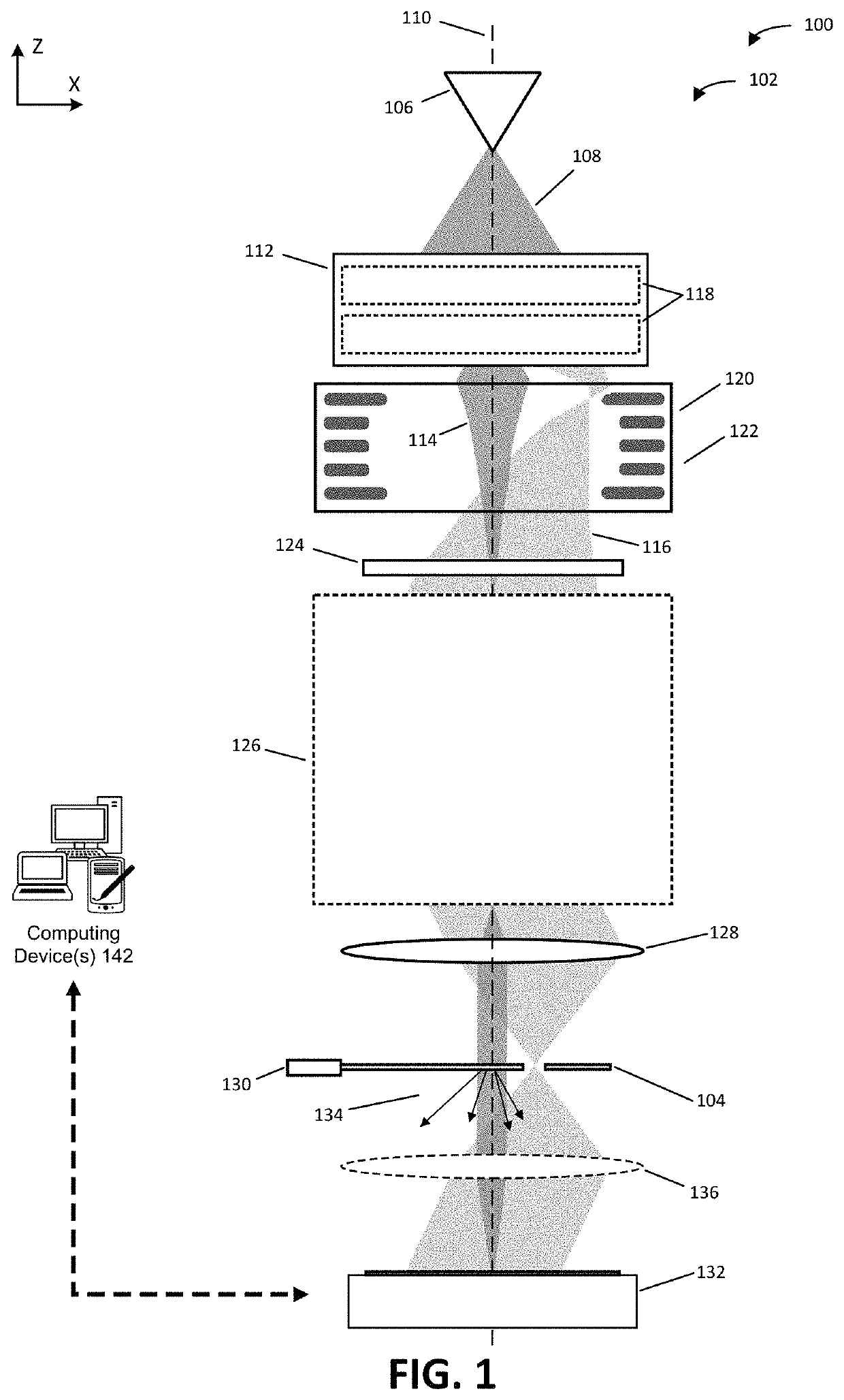
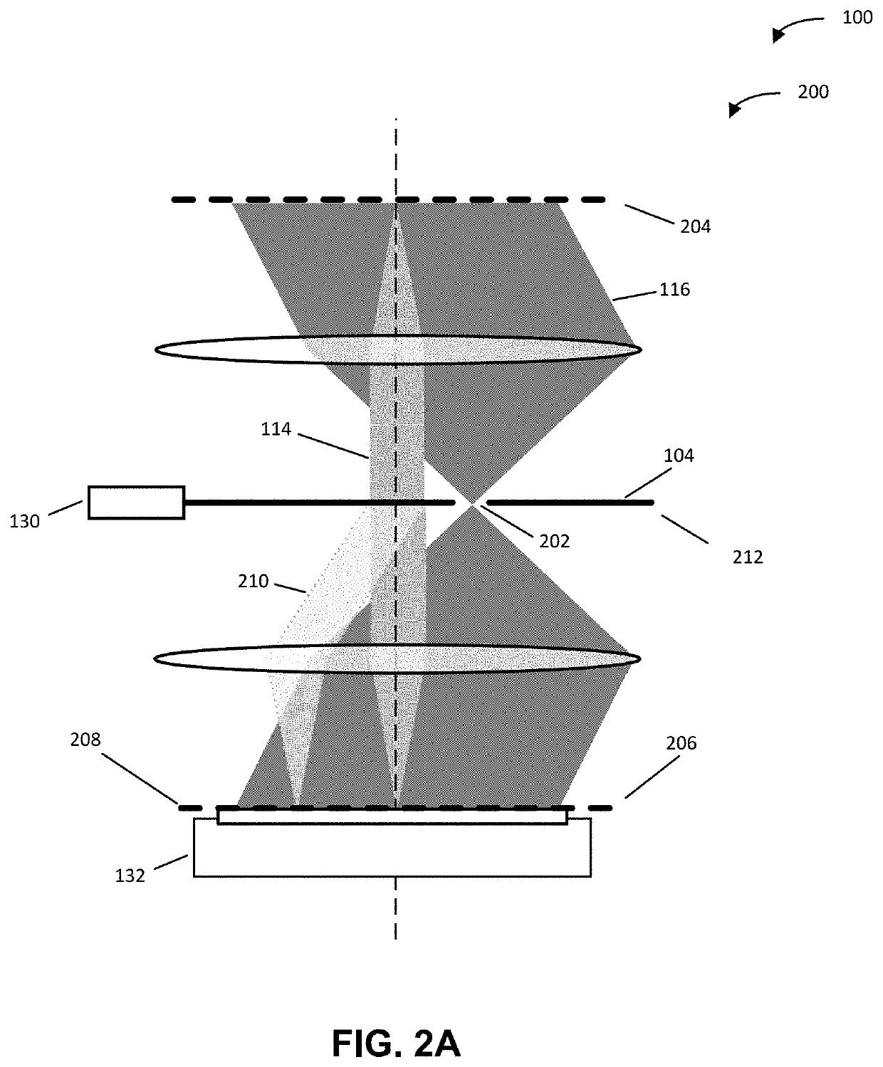
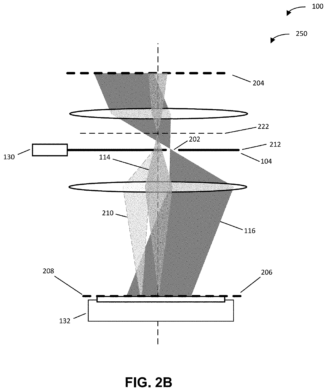
[0024]Methods and systems for performing electron diffraction holography, are included herein. More specifically, the methods and systems disclosed herein include and / or are configured to allow for diffraction holograms of a sample to be generated from interference patterns between an in-focus electron beam and a wide reference electron beam that are detected in the diffraction plane. In the methods and systems, a plurality of electrons that have been emitted by an electron source are split into a coherent first and second electron beam, and the focal properties of at least one of the first electron beam and the second electron beam are modified such that corresponding focal planes of the first electron beam and the second electron beam are different. In some embodiments, the focal plane of at least one of the first electron beam and the second electron beam is modified such that the first electron beam is focused at a plane at or near the sample, and the second electron beam is mad...


PUM

PropertyMeasurementUnit
radius RE1aaaaaaaaaa
voltagesaaaaaaaaaa

Abstract

Methods for using electron diffraction holography to investigate a sample, according to the present disclosure include the initial steps of emitting a plurality of electrons toward the sample, forming the plurality of electrons into a first electron beam and a second electron beam, and modifying the focal properties of at least one of the two beams such that the two beams have different focal planes. Once the two beams have different focal planes, the methods include focusing the first electron beam such that it has a focal plane at or near the sample, and focusing the second electron beam so that it is incident on the sample, and has a focal plane in the diffraction plane. An interference pattern of the first electron beam and the diffracted second electron beam is then detected in the diffraction plane, and then used to generate a diffraction holograph.

Description

CROSS REFERENCE TO RELATED APPLICATIONS[0001]This application relates to patent application Ser. No. 16 / 834,963, filed on Mar. 30, 2020, titled “Dual Beam Bifocal Charged Particle Microscope”, by Henstra et al., which is incorporated herein by reference in its entirety and for all purposes.BACKGROUND OF THE INVENTION[0002]A transmission electron microscope can be operated in Selected Area Electron Diffraction (SAED) mode, in which the diffraction plane is imaged onto a camera. This mode is especially useful for the study of crystalline material, in which case crystallographic information can be obtained. In the case where a single (monocrystalline) crystal is studied, diffraction patterns can even be used for the reconstruction of the 3D potential distribution of the atoms that constitute the crystal. For isotropic resolution, diffraction patterns need to be collected for all orientations of the crystal. In practice, data is usually collected while continuous tilting of the crystal ...

Claims


Application Information

Patent Timeline
Patent Type & Authority Patents(United States)
IPC IPC(8): G01N23/20G01N33/38G03H5/00H01J37/04H01J37/26G01N23/207
CPCG01N23/207G01N33/385G03H5/00H01J37/04H01J37/26G01N2223/0566G01N2223/064G03H2224/04H01J2237/2614G01N23/20058H01J37/295H01J37/21G01N2223/056G01N2223/102H01J2237/0492H01J2237/15H01J37/147H01J37/10H01J37/28G01N21/453G01N15/1459
Inventor HENSTRA, ALEXANDERDENG, YUCHENKOHR, HOLGER
Owner FEI CO
Why Eureka
Try Eureka