Semiconductor device and method for making the same

a technology of semiconductor devices and semiconductors, applied in semiconductor devices, semiconductor/solid-state device details, electrical apparatus, etc., can solve problems such as framing being susceptible to heat, memory operation becoming unstable, and memory no longer operating

Inactive Publication Date: 2001-06-07
ROHM CO LTD
View PDF1 Cites 15 Cited by
  • Summary
  • Abstract
  • Description
  • Claims
  • Application Information

AI Technical Summary

Benefits of technology

0011] It is therefore an object of the present invention to provide a semiconductor device in which the electrode of the semiconductor chip and the component element to be connected with the electrode are connected appropriately with each other without damaging a property of the semiconductor chip.

Problems solved by technology

If the FRAM containing such a ferroelectrics is heated to this Curie temperature or above, the memory operation becomes unstable, or the memory will no longer operate.
In other words, the FRAM is susceptible to heat.
However, this method is not suitable for wirebonding to a semiconductor chip which is susceptible to heat, because the semiconductor chip has to be heated up to 400 degrees Celsius.
However, the ultrasonic bonding method is disadvantageous in that an intense ultrasonic wave can break the wire.
Still however, the thermosonic bonding is only suitable for wirebonding a common type of semiconductors because the semiconductor chip must be heated to about 200 degrees Celsius.
The thermosonic bonding is still not suitable for wirebonding a semiconductor chip such as the FRAM which is extremely susceptible to heat, becoming very unstable in operation if heated to 170-180 degrees Celsius.
There is another problem.
However, aluminum is easily oxidized to form a coat of oxide, which weakens the bond between the bonding pad and the wire.
This problem becomes more significant at a higher bonding temperature, and in order to remove the coat of oxide, the ultrasonic wave of a greater intensity must be applied at a risk of breaking the metal wire.

Method used


Image

  • Semiconductor device and method for making the same
  • Semiconductor device and method for making the same
  • Semiconductor device and method for making the same

Examples


Embodiment Construction

[0053] Preferred embodiments of the present invention will be described in specific details, referring to the accompanying drawings.

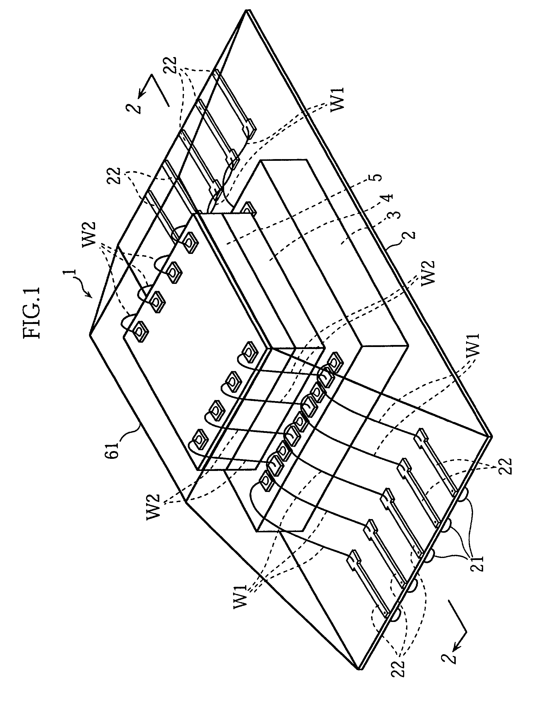
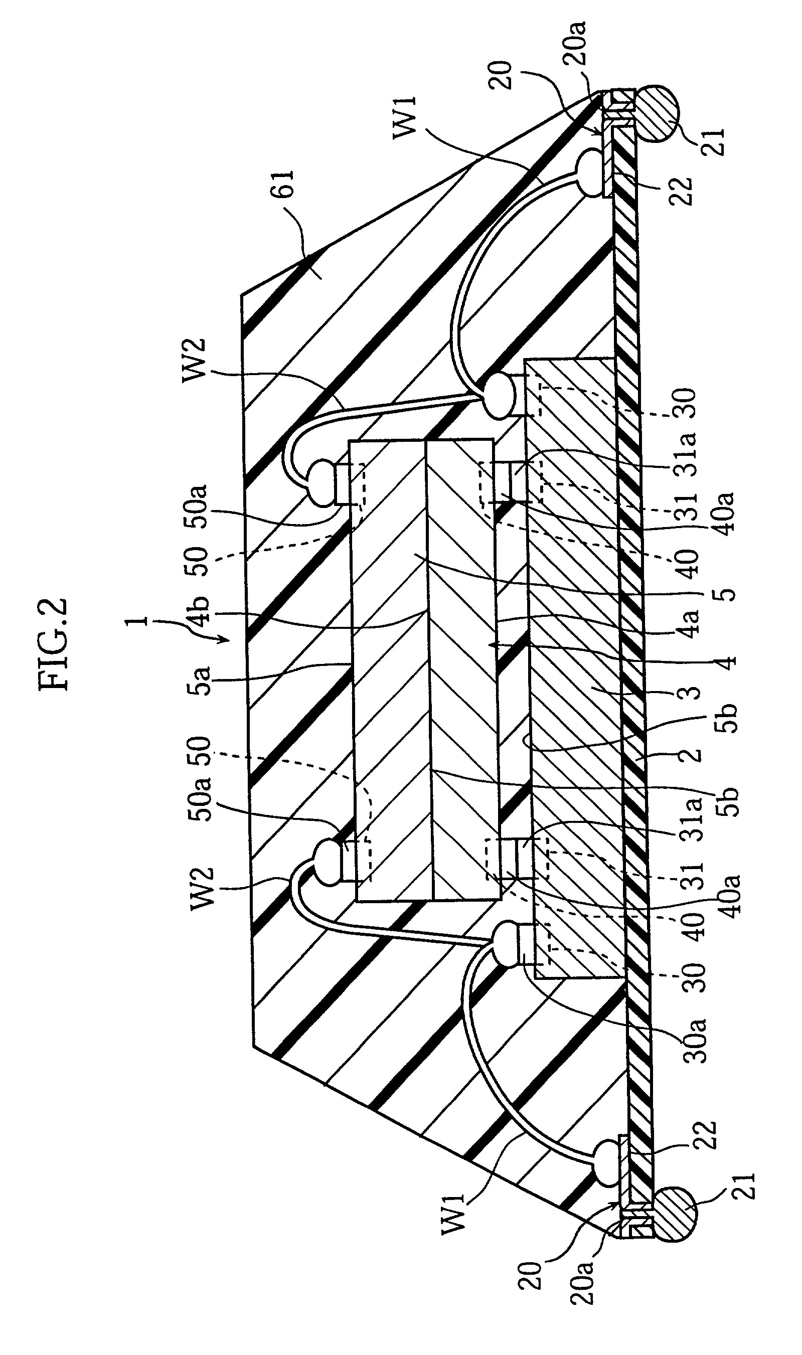
[0054] FIG. 1 is an overall perspective view of a semiconductor device as an embodiment of the present invention. FIG. 2 is a sectional view taken in lines 2-2 in FIG. 1.

[0055] As shown in FIGS. 1 and 2, a semiconductor device 1 generally comprises a film substrate 2 made of a polyimide resin for example, a first semiconductor chip 3 mounted to the film substrate 2, a second semiconductor chip 4 electrically connected with the first semiconductor chip 3, and a third semiconductor chip 5 mounted onto the second semiconductor chip 4.

[0056] The film substrate 2 has two end portions each formed with a plurality of through-holes 20a. At each of these through-holes 20a, a corresponding terminal 20 is formed. Each terminal 20 is provided with a thin-film terminal portion 22 formed on an upper surface of the film substrate 2, and a ball terminal portion 21 form...


PUM


Abstract

A semiconductor device includes a semiconductor chip having a main surface formed with an electrode pad, a package containing the semiconductor chip, a component element connected with the electrode pad within the package, a gold bump formed on the electrode pad, and a gold connecting member. The gold connecting member has an end bonded to the gold bump, and the other end bonded to the component.

Description

[0001] 1. Field of the Invention[0002] The present invention relates to a semiconductor device, and a method for making the same. More particularly, the present invention relates to a semiconductor device containing such a semiconductor chip as a ferroelectric random access memory which will become unstable in operation under a high temperature, and a method for making such a semiconductor device.[0003] 2. Background Art[0004] Much effort is being made in recent years in developing a nonvolatile memory utilizing the spontaneous polarization behavior of a ferroelectrics having a high dielectric constant. This type of memory is usually called the ferroelectric random access memory (hereinafter called FRAM). The FRAM has a construction in which a planer type ferroelectric capacitor is formed on a layer of a common CMOS transistor. The FRAM enables overwriting of stored information at an extremely high speed and at a low voltage by reversing the direction of polarization.[0005] However,...

Claims


Application Information

Patent Timeline
Patent Type & Authority Applications(United States)
IPC IPC(8): H01L23/31H01L25/065
CPCH01L23/3121H01L24/06H01L24/45H01L24/48H01L24/78H01L24/85H01L24/97H01L25/0657H01L2224/05624H01L2224/1134H01L2224/13144H01L2224/16145H01L2224/32145H01L2224/32225H01L2224/45144H01L2224/48091H01L2224/48145H01L2224/48227H01L2224/48465H01L2224/48475H01L2224/48624H01L2224/73265H01L2224/75251H01L2224/78301H01L2224/85051H01L2224/85181H01L2224/8592H01L2224/97H01L2225/06506H01L2225/0651H01L2225/06513H01L2225/06579H01L2225/06582H01L2225/06586H01L2924/01013H01L2924/01029H01L2924/01074H01L2924/01078H01L2924/01079H01L2924/01082H01L2924/014H01L2924/14H01L2924/15311H01L2924/19041H01L2924/01033H01L2224/0401H01L2224/11334H01L2924/00014H01L2224/83H01L2224/85H01L2924/00H01L2224/92247H01L2224/05554H01L2224/85203H01L2224/85205H01L2224/85207H01L2224/04042H01L2924/181H01L2924/10162H01L2224/85045H01L2224/78251H01L2924/00012H01L2224/4554
Inventor OKA, HIROSHIHIROMITSU, MASAAKI
Owner ROHM CO LTD
Why Eureka
Try Eureka