Color image display device, method of driving the same, and electronic equipment

a display device and color image technology, applied in the direction of driving chains, instruments, manufacturing tools, etc., can solve the problems of increasing the number of external input pins, increasing the occupied area of the driving circuit, and poor expression properties of accurate color

Inactive Publication Date: 2001-08-02
SEMICON ENERGY LAB CO LTD
View PDF7 Cites 41 Cited by
  • Summary
  • Abstract
  • Description
  • Claims
  • Application Information

AI Technical Summary

Problems solved by technology

However, in the case where a liquid crystal display device of high resolution and high definition is fabricated, forming the same number of D / A conversion circuits, each occupying a large area, as the source signal lines is an obstacle to the miniaturization of the liquid crystal display device which is desired in recent years, and a method of driving a plurality of source signal lines by one D / A conversion circuit is proposed in Japanese Patent Application Laid-open No. Hei. 11-167373.
At this time, there occur problems that G and B do not become sufficiently dark states, and the contrast becomes low, and further, an expression property for accurate color becomes poor.
These cause new problems such as an increase in the number of external input pins, and an increase in the occupied area of the driving circuit by a region for wiring of the gray-scale power supply lines, the added switch, and the like.

Method used


Image

  • Color image display device, method of driving the same, and electronic equipment
  • Color image display device, method of driving the same, and electronic equipment
  • Color image display device, method of driving the same, and electronic equipment

Examples


embodiment 1

[0065] Embodiment 1

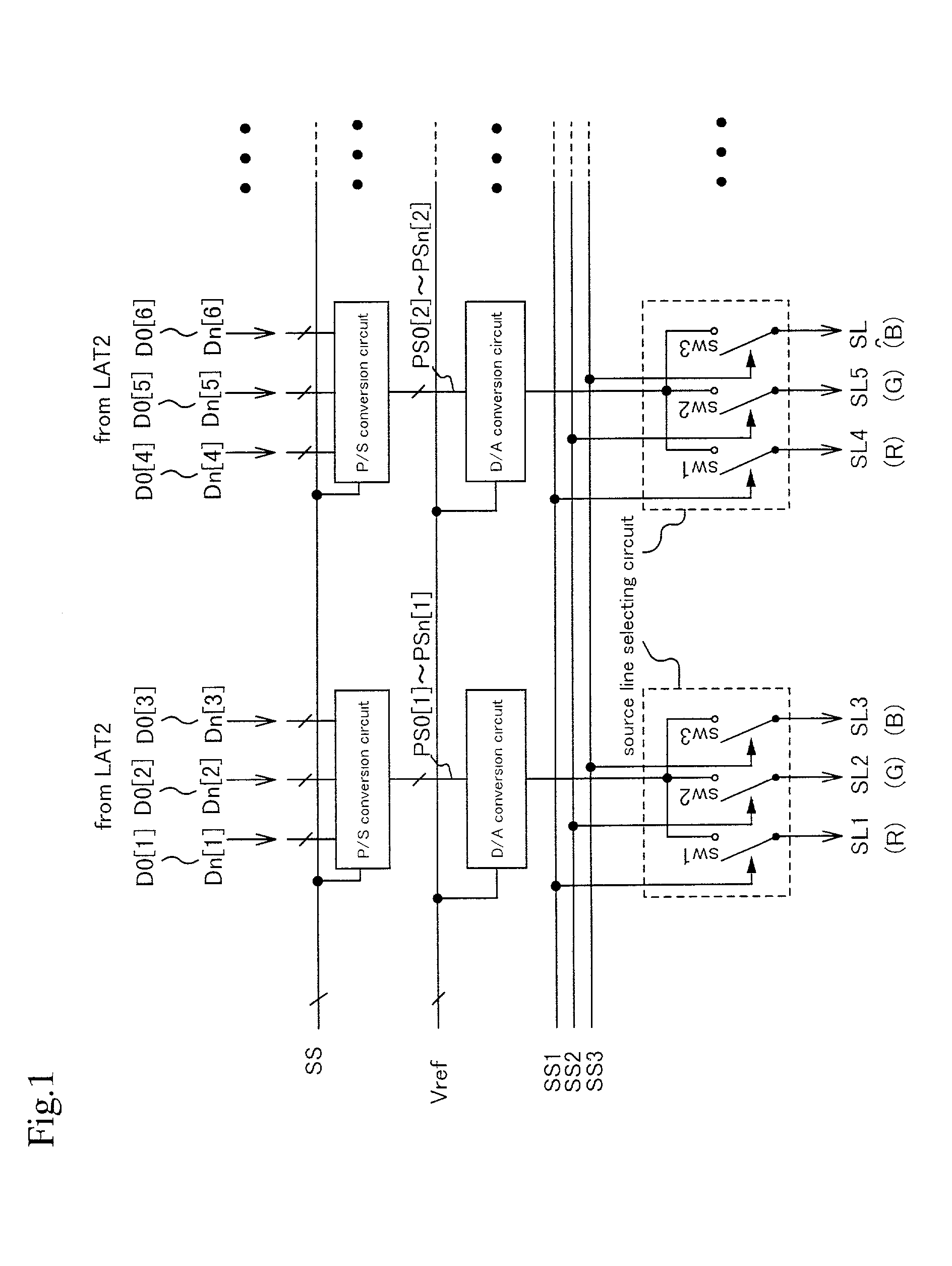
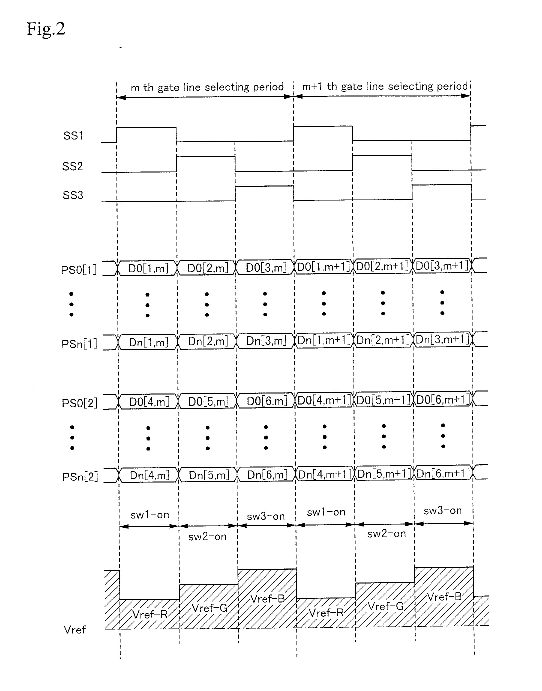
[0066] In this embodiment, an example in which the present invention is applied to an active matrix image display device will be described. As described in the related art, the active matrix image display device includes a source signal line driving circuit, a gate signal line driving circuit, and a pixel array portion disposed in a matrix form. Since the operations of the gate signal line driving circuit and the pixel array portion are the same as the related art, in this embodiment, the source signal line driving circuit will be described. Besides, as shown in FIG. 3, in this embodiment, a description will be made on a case, as an example, where a digital picture signal to the respective colors of RGB has 3 bits, and one D / A conversion circuit drives three source signal lines.

[0067] A shift register portion includes flipflop circuits (FF), NAND circuits, and inverter circuits, and a clock signal (CLK), an inversion clock signal (CLKb) of the clock signal, and a ...

embodiment 2

[0081] Embodiment 2

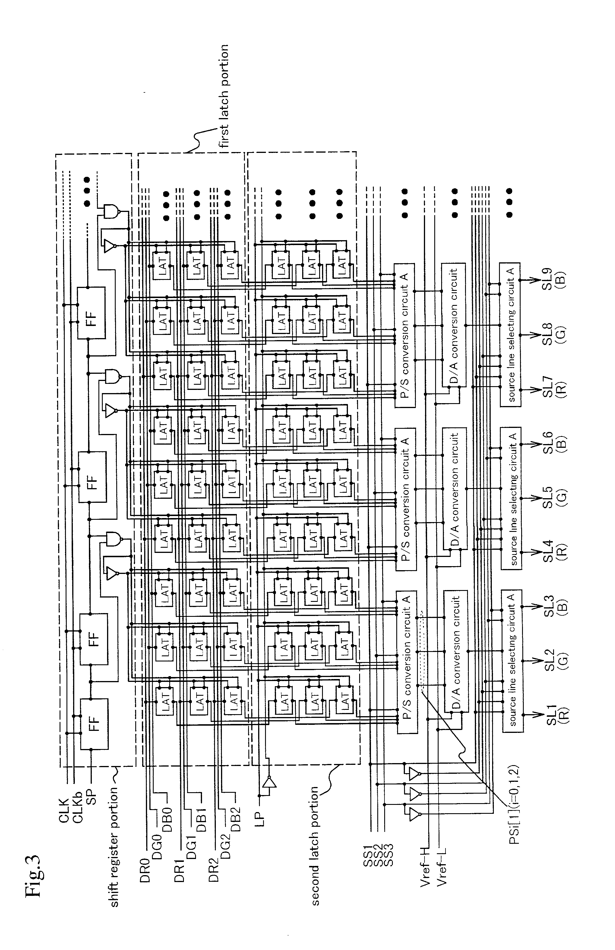
[0082] Also in this embodiment, similarly to the embodiment 1, an example in which the present invention is applied to an active matrix image display device will be described. However, differently from the embodiment 1, a description will be made on an example in which one D / A conversion circuit drives six (RGB.times.2) source signal lines. Also in this embodiment, a source signal line driving circuit will be mainly described. A shift register portion, a first latch portion, and a second latch portion are made the same as the embodiment 1, and their explanations are omitted below. FIG. 8 shows an example of structures of downstream circuits of a second latch circuit in this embodiment. Also in this embodiment, it is assumed that a digital picture signal for the respective colors of RGB has 3 bits.

[0083] Three (number of bits).times.six (RGB.times.2, that is, for six source signal lines) digital picture signals stored in the second latch portion and selecting signa...

embodiment 3

[0094] Embodiment 3

[0095] In this embodiment, as an example of a fabricating method in a case where the embodiment 1 and the embodiment 2 are applied to an active matrix liquid crystal display device, a method of fabricating a pixel TFT as a switching element of a pixel portion and a TFT of a driving circuit (source signal line driving circuit, gate signal line driving circuit, etc.) provided at the periphery of the pixel portion on the same substrate will be described in detail in accordance with its steps. However, for simplification of the explanation, a CMOS circuit which is a basic structural circuit in a driving circuit portion is shown, and n-channel TFT is shown in a pixel TFT portion.

[0096] In FIGS. 11A, an alkali-free glass substrate, for example, a 1737 glass substrate by Corning Inc. is used as a substrate 401. An under film 402 is formed by a plasma CVD method or a sputtering method on a surface of the substrate 401 over which a TFT is to be formed. As the under film 40...


PUM

PropertyMeasurementUnit
thicknessaaaaaaaaaa
thicknessaaaaaaaaaa
thicknessaaaaaaaaaa

Abstract

A gray-scale power supply line supplied to a source signal line driving circuit is made only one system, and each of D/A conversion circuits drives source signal lines in which three source signal lines corresponding to RGB are made a unit and the number of which is a multiple of 3. The periods in which respective source line selecting circuits select source signal lines corresponding to respective colors of the RGB are made synchronous with each other, and the power supply voltage applied to the gray-scale power supply line is changed in one horizontal writing period, so that power supply voltages corresponding to R, G and B are respectively applied to the gray-scale power supply line in periods while the source signal lines of R, G and B are respectively selected.

Description

[0001] 1. Field of the Invention[0002] The present invention relates to a color image display device (active matrix color image display device) in which information such as a picture image is displayed by switching elements and pixels arranged in a matrix form, particularly to a digital system driving method and an image display device using the same, and to an electronic equipment.[0003] 2. Description of the Related Art[0004] In recent years, a technique of fabricating a semiconductor device including a semiconductor thin film formed on an inexpensive glass substrate, for example, a thin film transistor (TFT), has been rapidly developed. The reason is that the demand for an active matrix image display device has increased.[0005] The active matrix image display device includes an active matrix liquid crystal image display device using liquid crystal for a display element, an EL display device using an electro luminescence (EL) element, and the like. Hereinafter, as a typical exampl...

Claims


Application Information

Patent Timeline
Patent Type & Authority Applications(United States)
IPC IPC(8): G09G3/20G09G3/32G09G3/36H01L21/77H01L21/84H01L27/12
CPCG09G3/20G09G3/2011G09G3/3233G09G3/3275G09G3/3688G09G2300/0426G09G2300/0465G09G2300/08G09G2300/0842G09G2300/0861G09G2310/0235G09G2310/0251G09G2310/027G09G2310/0297G09G2320/0233G09G2320/0238G09G2320/0242G09G2320/0673H01L27/12H01L29/4908H01L27/1277
Inventor AZAMI, MUNEHIRO
Owner SEMICON ENERGY LAB CO LTD
Why Eureka
Try Eureka