Semi-sacrificial diamond for air dielectric formation

a dielectric formation and semi-sacrificial diamond technology, applied in the field of very high density multi-level interconnected electronic structures, can solve problems such as crosstalk and capacitative coupling, short circuit risk,

Inactive Publication Date: 2001-08-16
IBM CORP
View PDF0 Cites 80 Cited by
  • Summary
  • Abstract
  • Description
  • Claims
  • Application Information

AI Technical Summary

Problems solved by technology

Increased also are problems associated advanced IC miniaturization and the attendant closer proximity of ...

Method used


Image

  • Semi-sacrificial diamond for air dielectric formation
  • Semi-sacrificial diamond for air dielectric formation
  • Semi-sacrificial diamond for air dielectric formation

Examples


second embodiment

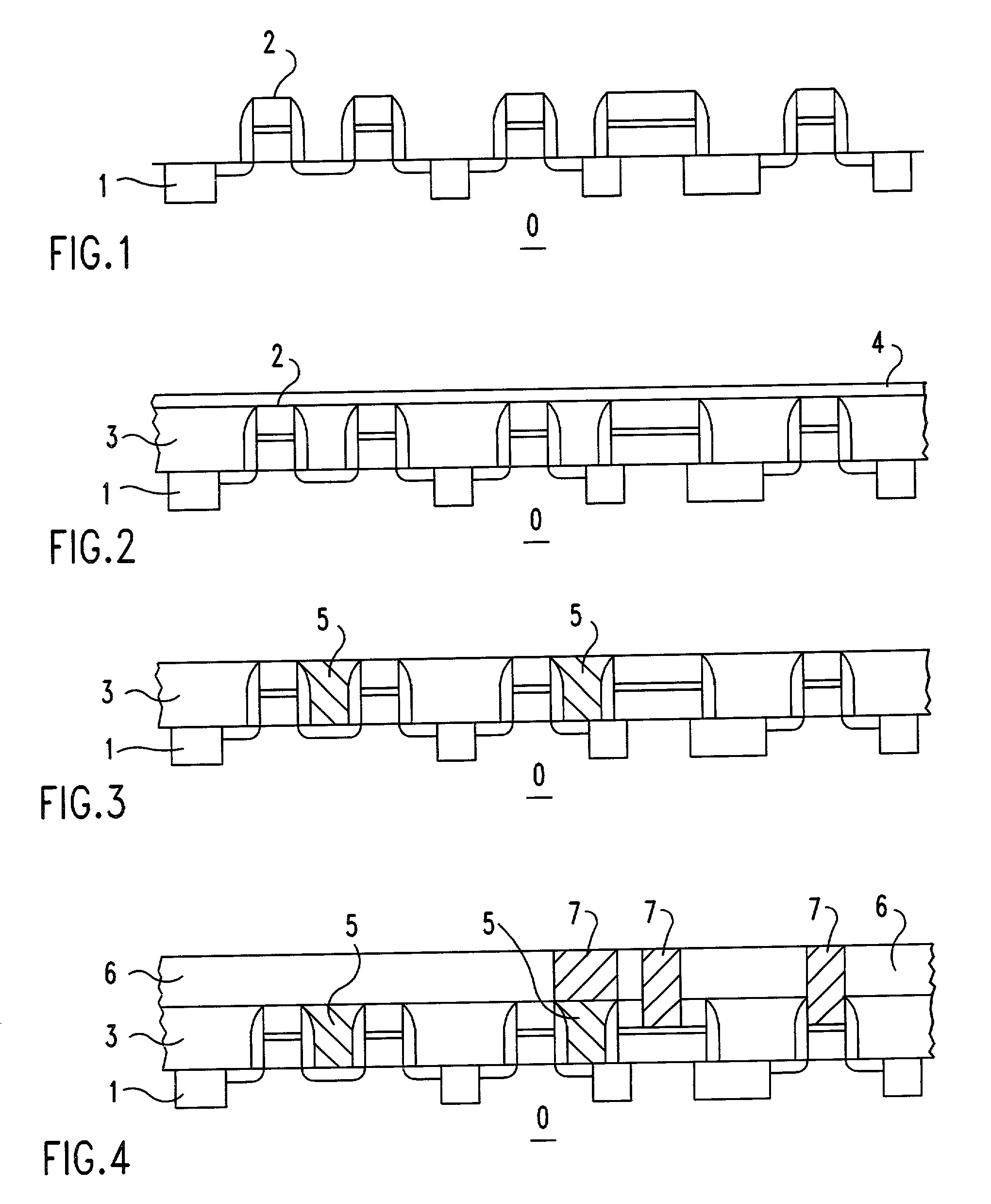
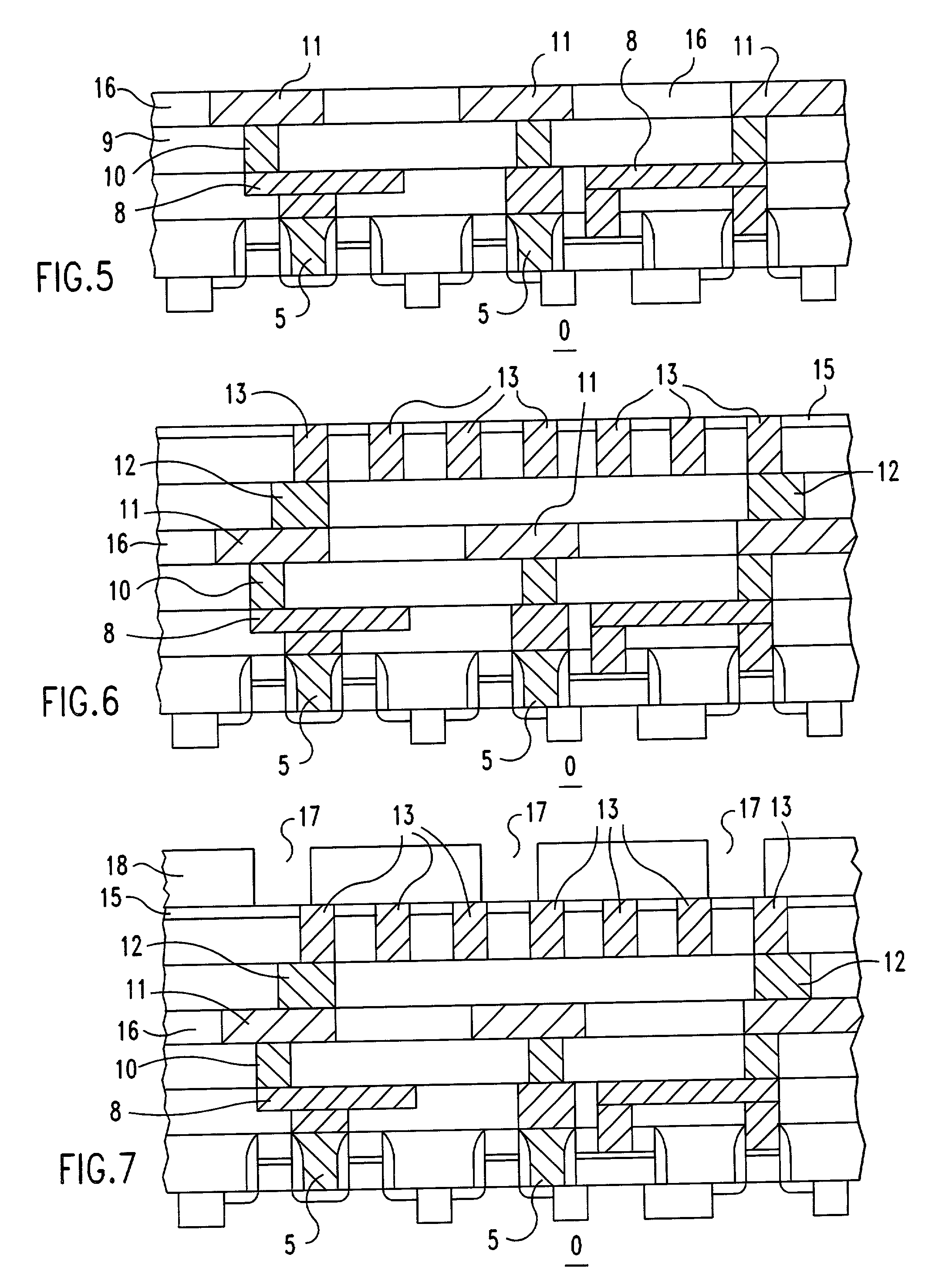
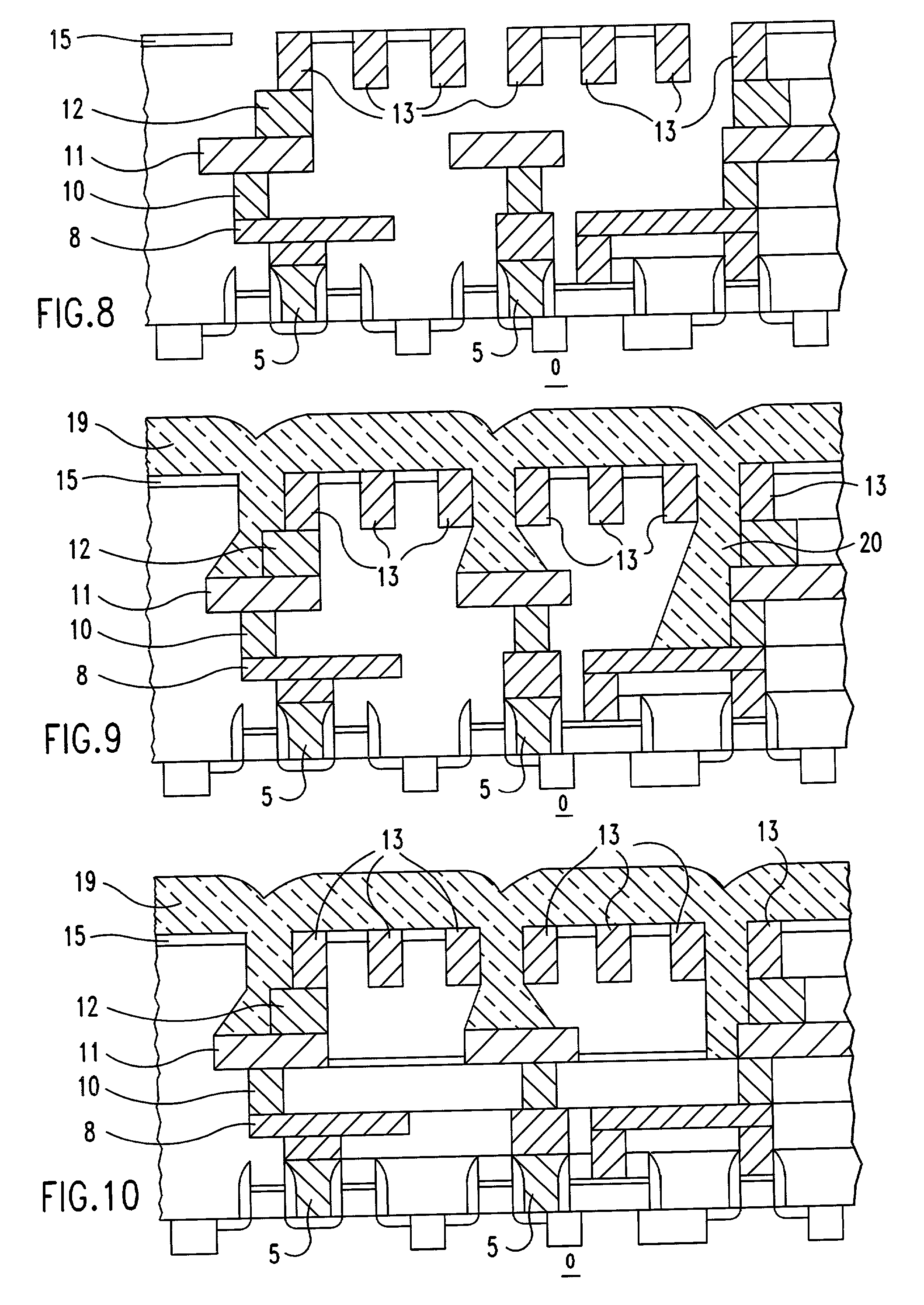
[0043] FIGS. 1-8 described above combined with FIG. 9 represent the present invention. When steps 1-8 are completed, A permanent cap of CVD diamond (19) is deposited onto the chip as represented in FIG. 9. The CVD diamond of the cap (19) is also deposited into the chip structure through the openings (17) in the hard mask (15), selectively sealing off lower interconnection levels from the ambient external to the chip. What is not shown is that by choice of layout the sides of the chip are also sealed. If the CVD diamond cap (19) is deposited in the atmosphere of an inert gas, such as argon or helium, that gas will be sealed within the chip rather than another. A sealed structure provides a more consistent dielectric medium by preventing the introduction of contaminants such as dirt of moisture from outside. The CVD diamond cap (19) also provides improved thermal conductivity, a factor which becomes more important as the structure becomes more complex and increased heat is generated d...

third embodiment

[0044] FIGS. 1-8 described above combined with FIG. 10 represent the present invention.

[0045] In the third embodiment of the present invention the steps represented in FIGS. 1-8 have been completed. Rather than removing all CVD diamond from horizontal levels in the structure as shown in FIG. 8, however, the diamond is incompletely etched out from the lower levels of the chip, leaving some remaining in regions of relatively lower pattern density. In FIG. 9, CVD diamond levels (9), (16) and CVD diamond located in second via level (12) are shown to be incompletely etched out. A partial removal provides improved mechanical stability and thermal conductivity, especially in structures having many levels, while maintaining the benefit of low dielectric air gaps in regions of relatively higher pattern density at the upper levels as shown in FIG. 10. The intent is to have diamond in those areas where more mechanical support to the structure is required and to have air dielectric in those are...


PUM


Abstract

Disclosed is a structure and process for incorporating air or other gas as a permanent dielectric medium in a multilevel chip by providing CVD diamond as a semi-sacrificial interlevel and intralevel dielectric material. The semi-sacrificial dielectric is subsequently at least partially removed in an isotropic oxygen etch. A variation of the disclosure includes providing a final, permanent CVD diamond encapsulant to contain the gaseous dielectric medium within the chip.

Description

[0001] 1. Field of the Invention[0002] This invention relates to high density integrated circuit (IC) devices. More particularly, this invention relates to very high density multilevel interconnect electronic structures, and processes of fabricating such structures, which are comprised of alternating via levels and wiring levels embedded in a gas dielectric medium, suitable for mounting on carriers such as multichip modules.[0003] 2. Background Art[0004] The continuing drive toward reduction in dimensions and increase in the number and density of components within IC chips is inspired by increasingly more aggressive requirements of memory and logic. Smaller chip features provide higher bit density, lower operating voltages, lower energy consumption and faster device speed. Increased also are problems associated advanced IC miniaturization and the attendant closer proximity of circuit features to one another, including risk of shorting, crosstalk and capacitative coupling, among othe...

Claims


Application Information

Patent Timeline
IPC IPC(8): H01L21/768
CPCG06Q10/0639G06Q40/04H01L21/7682
Inventor CLEVENGER, LAWRENCE A.HSU, LOUIS LU-CHEN
Owner IBM CORP
Why Eureka
Try Eureka