Test interface circuit and semiconductor integrated circuit device including the same

a technology of integrated circuits and test interfaces, which is applied in the direction of measurement devices, digital storage, instruments, etc., can solve the problems of large load, inability to accurately perform test of dram operation timing margins, and difficulty in ensuring the reliability of drams

Inactive Publication Date: 2001-08-23
RENESAS ELECTRONICS CORP
View PDF0 Cites 50 Cited by
  • Summary
  • Abstract
  • Description
  • Claims
  • Application Information

AI Technical Summary

Problems solved by technology

However, the logic performs control for carrying out the test, and therefore has to bear a large load.
Thus, the function test of DRAM is executed via the logic so that tests of, e.g., an operation timing margin of the DRAM cannot be performed accurately.
Further, from a viewpoint of a program capacity, the logic can generate only a limited number of test patterns so that the test cannot be performed sufficiently, and it is difficult to sufficiently ensure the reliability of the DRAM.
As a gate scale of the logic increases, the probability of occurrence of a failure in the logic itself increases so that the reliability of the memory test lowers.
When the data of 256 bits is directly applied to the external memory tester, data processing on the memory tester side becomes extremely difficult, and in addition the number of test data I / O pins increases to 512 (=256.times.2), which is not an available value in view of practical use.
However, the large scale logic LG in the DRAM-embedded system LSI performs input / output of many signals for system interface with an external device, and therefore large scale logic LG requires a large number of external pin terminals.
Therefore, it may possibly be impossible to allocate a sufficient number of external pin terminals to test interface circuit TIC for externally and directly testing the DRAM core.
However, if the bidirectional I / O circuit is used for transferring the test data to and from DRAM core MCR via test interface circuit TIC, conflict occurs between the test input data and the test output data, and therefore DRAM core MCR cannot be tested at a practical operation speed.
Even if output enable signal OE is set to L-level in response to falling of test clock signal TCLK in clock cycle #4, switching of the input / output I / O circuits is not performed adequately in clock cycle #4, and it is impossible for test interface circuit TIC to take in test data for application in a stable manner.
Accordingly, in the case where the test data output terminals and the test data input terminals commonized for reducing the number of the test pin terminals, it is impossible to perform tests of successive operations (e.g., read-write-read-write) in accordance with the page mode, and it is substantially impossible to perform the test on the DRAM core at the practical speed.

Method used


Image

  • Test interface circuit and semiconductor integrated circuit device including the same
  • Test interface circuit and semiconductor integrated circuit device including the same
  • Test interface circuit and semiconductor integrated circuit device including the same

Examples


Embodiment Construction

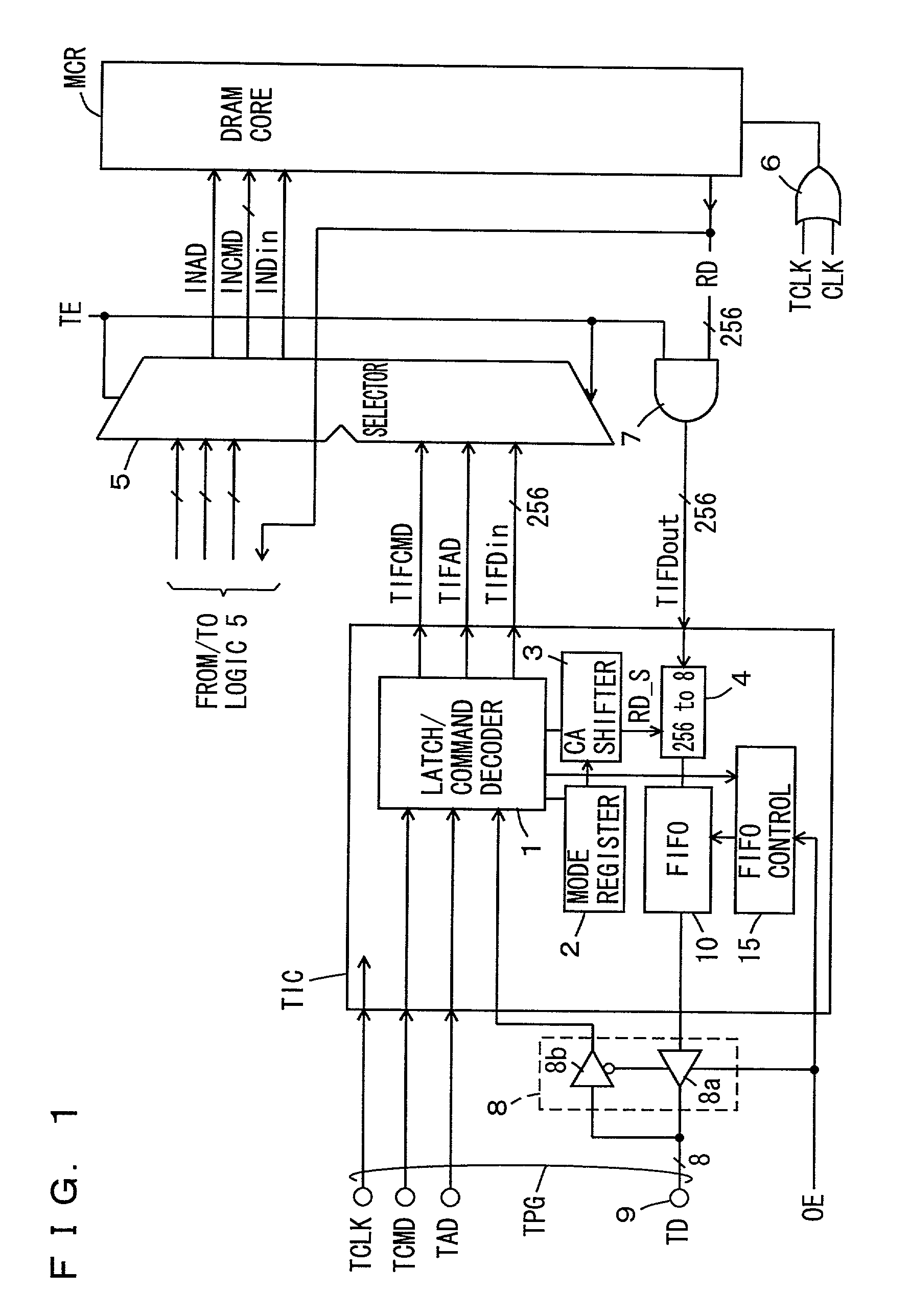
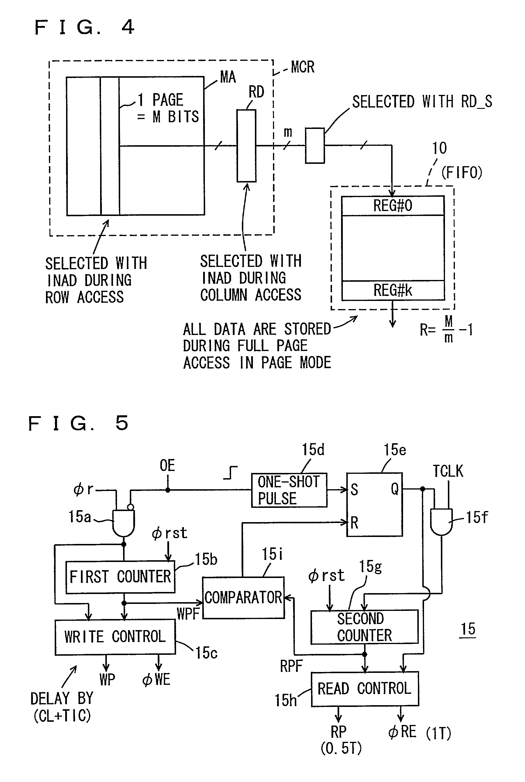
[0128] One page in the embedded DRAM may have a size other than 2048 bits. The input / output data of the DRAM core may have a bit width m of, e.g., 128 bits or 512 bits other than the foregoing value.

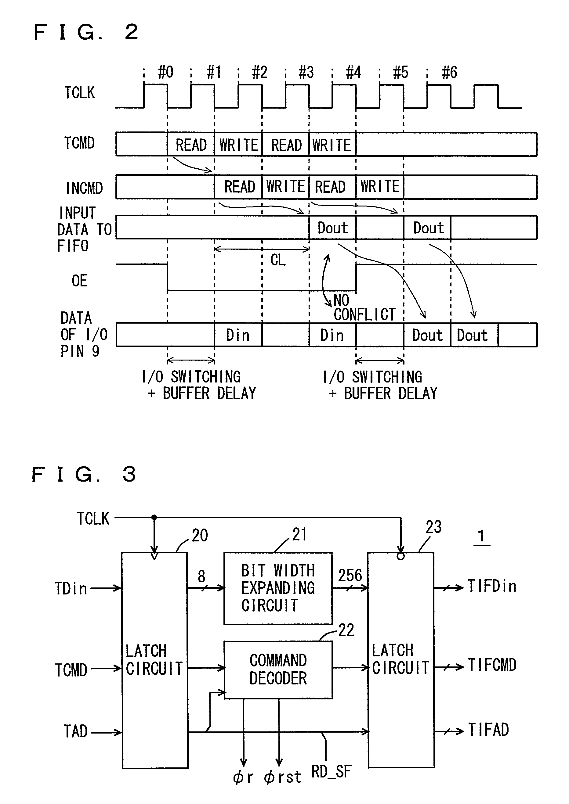
[0129] Column latency CL may take a value other than 2. If delay of the input data in the bidirectional I / O circuit cannot be neglected, the data write timing of the first-in first-out circuit is adjusted considering this delay.

[0130] The memory is not restricted to the DRAM, and may be another kind of memory such as a burst SRAM (Static Random Access Memory) or a flash memory, which operates in synchronization with the clock signal. The invention can be applied to any memory, provided that the memory is integrated with a logic on the same semiconductor substrate.

[0131] As described above, the invention can provide the test interface circuit, which allows a sufficient test on a mixed (embedded) memory without constraints on the test patterns due to the test data input / output switching ti...


PUM


Abstract

In a test interface circuit arranged between an embedded memory and a test data input/output (I/O) terminal, a first-in first-out circuit for successively storing test data is arranged for controlling a latency of data read from the embedded memory. The test interface circuit for the embedded memory can reduce the number of test data I/O terminals, and can increase the executable test patterns.

Description

[0001] 1. Field of the Invention[0002] The present invention relates to a test interface circuit and a semiconductor integrated circuit device using the same, and particularly relates to a test interface circuit for externally and directly testing a logic-merged memory as well as a semiconductor integrated circuit device including the same.[0003] 2. Description of the Background Art[0004] In a system LSI such as a logic-merged DRAM, in which a logic such as a processor or an ASIC (Application Specific Integrated Circuit) and a Dynamic Random Access Memory (DRAM) of a large storage capacity or the like are integrated on a common semiconductor chip (semiconductor substrate), the logic and the DRAM are interconnected via an internal data bus of multiple bits from 128 bits to 512 bits for achieving a data transfer rate faster by one, two or more orders than that of a general-purpose DRAM. The DRAM and the logic are interconnected via internal interconnection lines, which are much shorte...

Claims


Application Information

Patent Timeline
Patent Type & Authority Applications(United States)
IPC IPC(8): G01R31/28G01R31/317G01R31/3185G11C7/00G11C29/00G11C29/02
CPCG01R31/3172G01R31/31723G11C29/1201G11C29/12015G11C29/14G11C29/28G11C29/48G11C2029/0401
Inventor ARIMOTO, KAZUTAMISHIMANO, HIROKI
Owner RENESAS ELECTRONICS CORP
Why Eureka
Try Eureka