Method for fabricating electronic circuit device, semiconductor device and electronic circuit device

a technology of electronic circuit device and semiconductor device, which is applied in the direction of semiconductor device, semiconductor device details, electrical apparatus, etc., can solve the problems of not all bumps can be bonded, cracks may occur at the bonding portion of bump bonding, and serious mechanical damage does not occur

Inactive Publication Date: 2001-12-13
SONY CORP
View PDF0 Cites 18 Cited by
  • Summary
  • Abstract
  • Description
  • Claims
  • Application Information

AI Technical Summary

Problems solved by technology

However, when the amplitude of ultrasonic vibration is increased, the pressure imposed on the semiconductor device is increased, or the application time of ultrasonic vibration is lengthened to raise the bump bonding strength as described above, there is a danger that crack may occur at the bonding portion of a bump bonding.
In the related art, however, in semiconductor devices with a number of bumps arranged in any shape, there was a disadvantage that not all bumps can be bonded under the condition that the bonding strength is higher than a desired value and serious mechanical damages do not occur
On the contrary, if the bonding conditions are controlled so that cratering does not occur for all bumps, sufficient bonding strength cannot be attained for bumps arranged along the sides parallel with the application direction of ultrasonic vibration.

Method used


Image

  • Method for fabricating electronic circuit device, semiconductor device and electronic circuit device
  • Method for fabricating electronic circuit device, semiconductor device and electronic circuit device
  • Method for fabricating electronic circuit device, semiconductor device and electronic circuit device

Examples


second embodiment

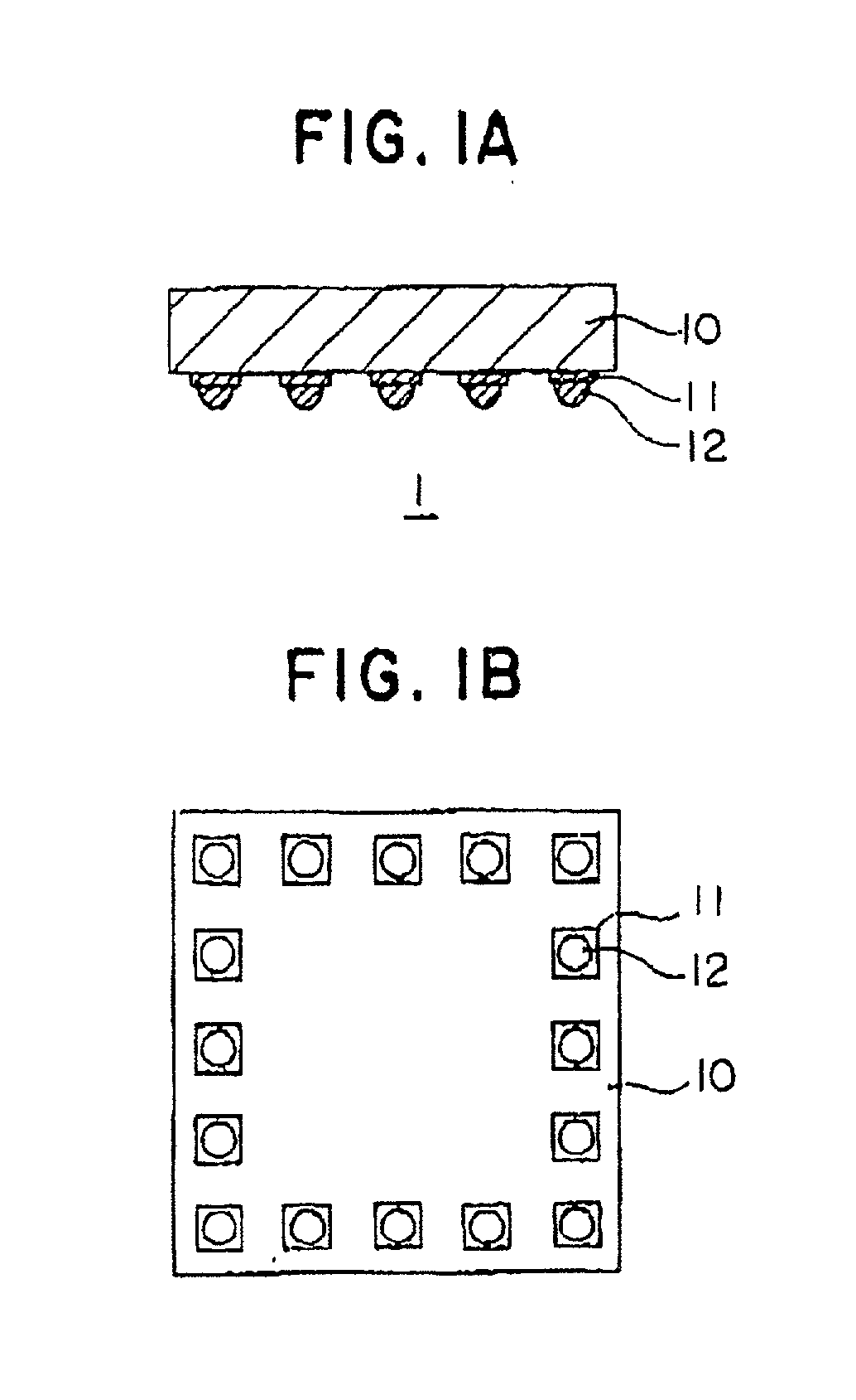
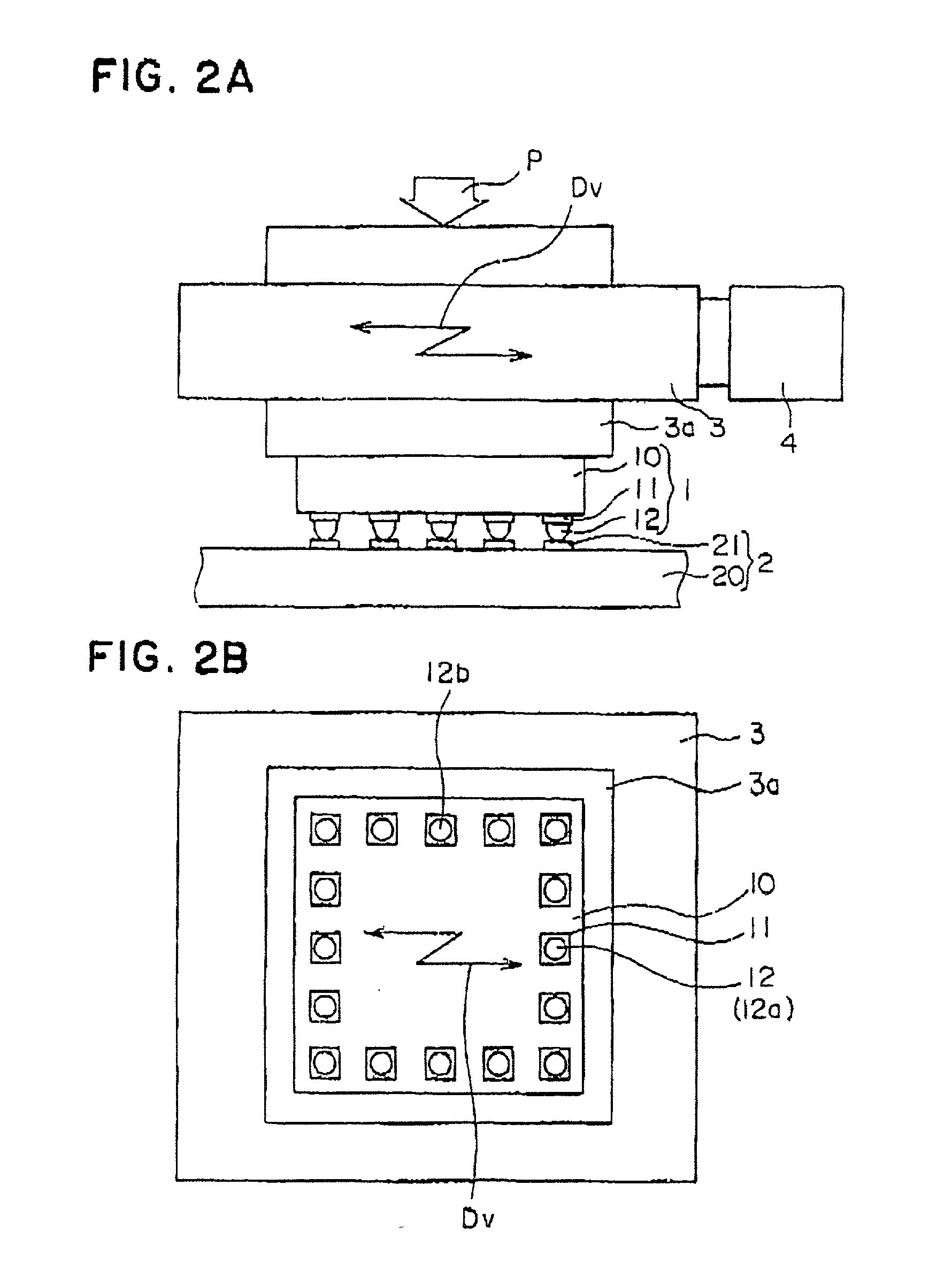
[0127] In the second embodiment, same as the first embodiment, a semiconductor device as shown in the sectional view of FIG. 1A and the plan view of FIG. 1B is to be mounted.

[0128] To surround the periphery of the electric circuit pattern of a semiconductor chip 10 of for example an area of 3 mm.times.3 mm and a thickness of 0.3 mm, pad electrodes 11 are formed of for example aluminum or others near the periphery so as to be connected with the electric circuit pattern.

[0129] The forming surface of the pad electrodes 11 is covered by a not shown surface protection film comprised of for example a silicon nitride film or a polyimide film, leaving openings at places where the pad electrodes 11 are located.

[0130] At these openings, bumps 12 are formed of gold or other conductive materials, and are arranged in square shapes as the arrangements in FIG. 9A. For example, in case of gold stud bump (gold 99.99%), bumps that are 70 to 80 .mu.m in diameter and about 50 .mu.m in height can be for...


PUM


Abstract

A method for fabricating an electric circuit device able to ensure bonding strength and bond bumps without occurrence of cratering or other mechanical damages The method for fabricating an electric circuit device wherein a semiconductor device having a plurality of bumps formed in an approximate polygonal shape or others on a semiconductor chip so as to be connected with the circuit pattern of a semiconductor chip is mounted on a mounting board including electrodes formed on a board made of glass-epoxy based or other materials, comprises steps of, first, aligning the bumps with the electrodes and placing the semiconductor device on the mounting board, then while pressing from the upside of the semiconductor device to make the bumps and electrodes contact closely, applying ultrasonic vibration to the semiconductor device with the application direction Dv to be the direction of a diagonal of the semiconductor chip or a direction not parallel with any side of the approximate polygon formed by the arranged bumps, and fusing the bumps and electrodes by the generated heat.

Description

[0001] 1. Field of the Invention[0002] The present invention relates to a method for fabricating an electric circuit device, and to a semiconductor device and an electric circuit device, more specifically, to a method for fabricating an electric circuit device including a semiconductor device having a package form of a small size and high density and mounted on a mounting board, and to a semiconductor device involved in the method, and an electric circuit device obtained with the same method.[0003] 2. Descriptions of the Related Art[0004] While requirements become stronger and stronger for reducing sizes, thicknesses and weights of digital video cameras, digital cellular telephones, or portable personal computers, or other portable electric apparatuses, recent VLSI semiconductor devices have been reduced by 30% in size during three years to respond to these requirements. On the other hand, it has been studied and developed as an important subject how the packing density of parts on ...

Claims


Application Information

Patent Timeline
Patent Type & Authority Applications(United States)
IPC IPC(8): H05K3/32H01L21/60H01L21/607H01L23/12
CPCH01L24/11H01L24/81H01L2924/13091H01L2224/13099H01L2224/13144H01L2224/16H01L2224/75H01L2224/757H01L2224/81801H01L2924/01004H01L2924/01013H01L2924/01015H01L2924/01029H01L2924/01039H01L2924/01074H01L2924/01078H01L2924/01079H01L2924/01082H01L2924/09701H01L2924/01005H01L2924/01006H01L2924/01019H01L2924/01033H01L2924/014H01L2924/00H01L24/05H01L2224/05568H01L2224/05573H01L2224/05624H01L2224/06135H01L2224/1134H01L2224/45144H01L2924/00014H01L23/12
Inventor IWAHASHI, SHINJISEKINE, JUNICHIYAMASAKI, HIROSHI
Owner SONY CORP
Why Eureka
Try Eureka