

Methods of forming self-aligned contact pads using a damascene gate process
a damascene gate and contact pad technology, applied in the direction of semiconductor devices, electrical equipment, transistors, etc., can solve the problems low resistance conductive material act coverage, and inability to ensure the reliability of the gate insulating layer, etc., to achieve excellent dummy gate profile, improve the effect of low resistance conductive material act coverage, and easy etching
- Summary
- Abstract
- Description
- Claims
- Application Information
AI Technical Summary
Benefits of technology
Problems solved by technology
Method used
Image

Examples
Embodiment Construction
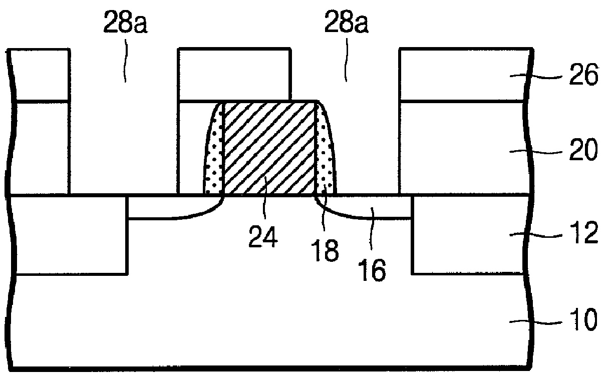
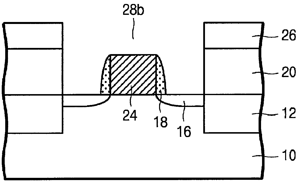
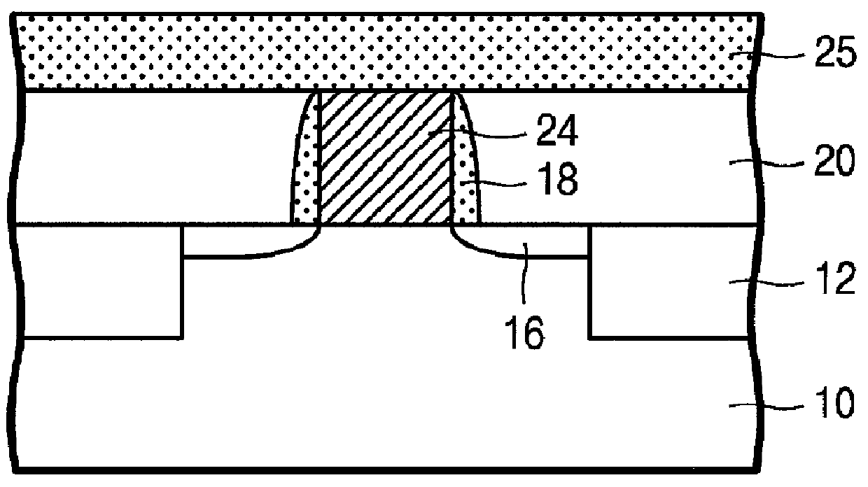
[0038] The present invention will now be described more fully hereinafter with reference to the accompanying drawings, in which preferred embodiments of the invention are shown. This invention may, however, be embodied in different forms and should not be construed as limited to the embodiments set forth herein. Rather, these embodiments are provided so that this disclosure will be thorough and complete, and will fully convey the scope of the invention to those skilled in the art. In the drawings, the thickness of layers and regions are exaggerated for clarity.
[0039] One standard photolithographic process includes creating a photolithography mask containing the pattern of the component to be formed, coating the wafer with a light sensitive material known as a photoresist, exposing the photoresist coated wafer to ultra-violet light through the mask to soften or harden parts of the photoresist (depending on whether positive or negative photoresist is used), removing the materials left...
PUM
 Abstract
Description
Claims
Application Information