
Process and structure for an interlock and high performance multilevel structures for chip interconnects and packaging technologies

a multi-level structure, interlocking technology, applied in the direction of cameras, instruments, cameras, etc., can solve the problems of wiring defects, blistering, other defects, voids or seams in the wiring,

Inactive Publication Date: 2002-01-31
IBM CORP
View PDF0 Cites 19 Cited by
  • Summary
  • Abstract
  • Description
  • Claims
  • Application Information

AI Technical Summary

Problems solved by technology

Both methods of deposition normally produce at best conformal deposits and inevitably lead to defects (voids or seams) in wiring especially when trenches have a cross section narrower at the top then at the bottom.
In electroless plating, while offering the advantage of low cost, the evolution of hydrogen during metal deposition tends to lead to blistering and other defects that are viewed as weaknesses for industry-wide implementation.

Method used


Image

  • Process and structure for an interlock and high performance multilevel structures for chip interconnects and packaging technologies
  • Process and structure for an interlock and high performance multilevel structures for chip interconnects and packaging technologies
  • Process and structure for an interlock and high performance multilevel structures for chip interconnects and packaging technologies

Examples


Embodiment Construction

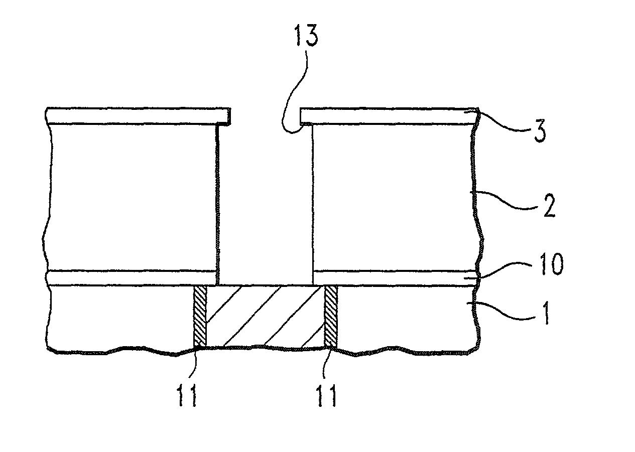
[0013] In order to facilitate an understanding of the present invention, the embodiment discussed will be directed to a Damascene plating process in which plating is carried out over a substrate such as a semiconductor, flat panel or packaging substrate.

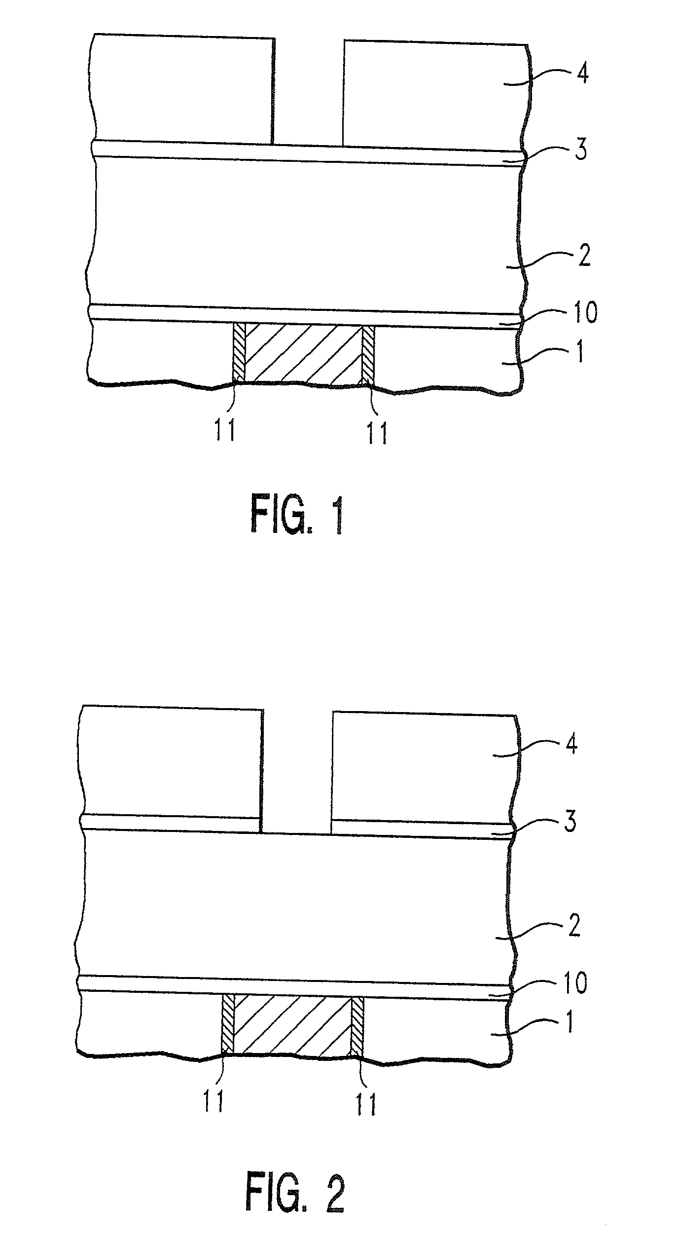
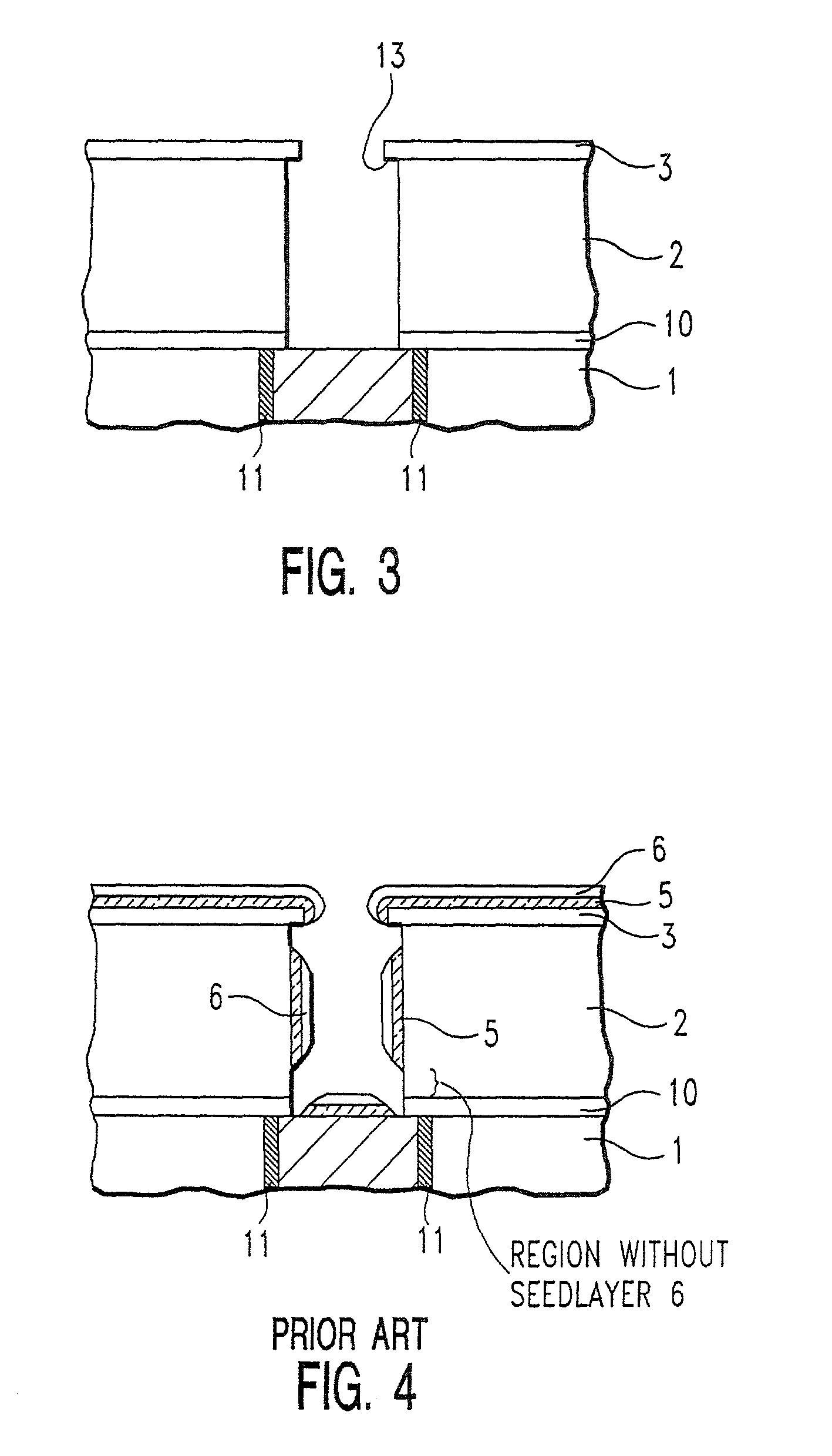
[0014] A schematic representation of the process of the present invention is illustrated in FIGS. 1-3 and 7-17.

[0015] In particular, a layer of a first dielectric 2 is deposited over the semiconductor substrate or wafer 1. See FIG. 1. The dielectric layer 2 typically has a dielectric constant of less than 4. However, for certain applications, the dielectric constant of the dielectric layer 2 is greater than 10. As illustrated in FIG. 1, also included between the substrate 1 and dielectric layer 2 is an interlevel dielectric layer 10. Also, the substrate 1 includes lower level wiring 11. The interlevel dielectric layer is typically a silicon dioxide, silicon nitride, silicon oxynitride or alumina.

[0016] The preferred dielectric layer ...


PUM

PropertyMeasurementUnit
dielectric constantaaaaaaaaaa
thickaaaaaaaaaa

Abstract

Method and structures for making a highly reliable metal interlock structure with continuous via and line structures. The absence of barrier layers between vias and lines or absence of interlevel dielectric layer is used to enhance chip performance.

Description

[0001] The present invention relates to a structure and a process for plating vias and lines and is particularly concerned with significantly reducing, if not entirely eliminating, void formation in the plating in the vias and lines. The present invention finds particular applicability in filling undercut features in interconnect and packaging structures.BACKGROUND OF INVENTION[0002] AlCu and its related alloy are currently the predominately used conductors for forming interconnection from electronic devices such as integrated circuits. The amount of Cu in AlCu is typically in the range from about 0.3 to 4%.[0003] Replacement of AlCu by Cu and Cu alloys as a chip interconnection material results in advantages of improved chip performance. Performances improved because the resistivity of Cu in certain copper alloys is less than the resistivity of AlCu. Besides performance, high chip yield count and higher circuit wiring density are also realized.[0004] The advantages of copper metall...

Claims


Application Information

Patent Timeline
Patent Type & Authority Applications(United States)
IPC IPC(8): C25D3/38H01L21/3205C25D5/48C25D7/12H01L21/288H01L21/768H01L23/532
CPCH01L21/2885H01L21/76843H01L21/76852H01L21/76862H01L21/76865H01L21/76873H01L21/76877H01L2924/0002H01L21/76885H01L23/53233H01L23/53238H01L2924/12044H01L2924/00G03B11/043G02B27/646H04N23/55H04N23/68
Inventor UZOH, CYPRIAN E.
Owner IBM CORP
Learn More