Organic electroluminescent device with improved hole injecting structure

Inactive Publication Date: 2002-01-31
CITYU RES
View PDF0 Cites 42 Cited by
  • Summary
  • Abstract
  • Description
  • Claims
  • Application Information

AI Technical Summary

Benefits of technology

0007] It is an object of the present invention to provide an OELD with an increased electroluminescen

Problems solved by technology

However, only very few patents have de

Method used


Image

  • Organic electroluminescent device with improved hole injecting structure
  • Organic electroluminescent device with improved hole injecting structure
  • Organic electroluminescent device with improved hole injecting structure

Examples


example 1

[0022] Fabrication Procedure

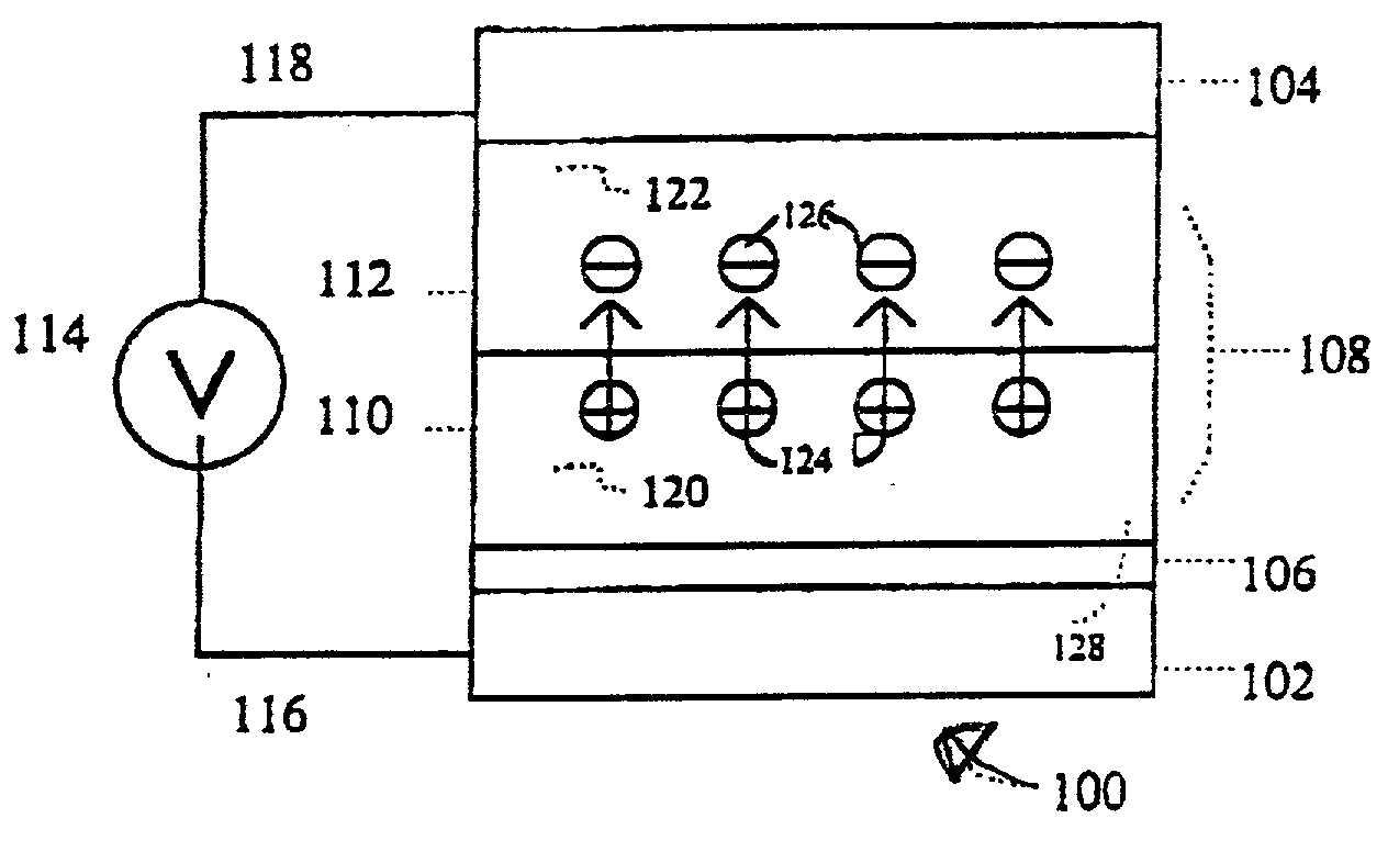
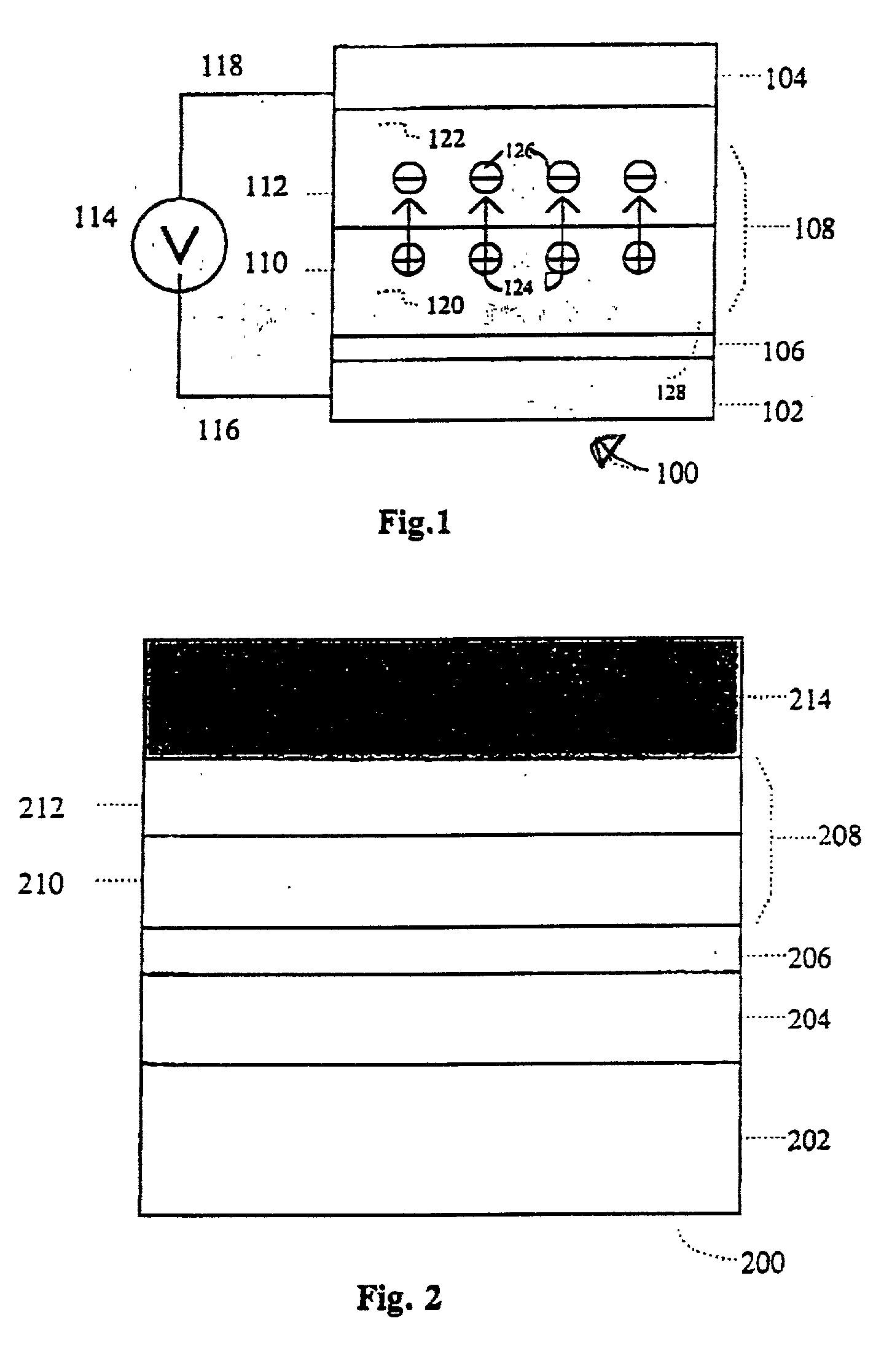
[0023] An OELD satisfying the requirements of the invention was constructed in the following manner. The device structure has an inorganic buffer layer and a two organic-layer stack, namely hole transporting layer and fluorescent emitting and electron transporting layer.

[0024] An indium-tin-oxide coated glass substrate was sequentially ultrasonicated in a commercial detergent, rinsed in deionized water, degreased in organic solvent, such as ethanol and acetone, and exposed to ultraviolet light and ozone for a few minutes.

[0025] An inorganic buffer layer (0-200 Angstroms) was then deposited on top of the ITO coated substrate by evaporation.

[0026] Onto the buffer layer was deposited a hole transporting layer of TPD or NPB (500-1,500 Angstroms), evaporated from a tantalum boat.

[0027] A fluorescent emitting and electron transporting layer of Alq (600 Angstroms) was then deposited onto the hole transporting layer.

[0028] On top of the Alq layer was deposited a ...

example 2

[0030] OELDs with SiO.sub.2 Buffer Layer

[0031] The OELDs were fabricated according to the procedure of Example 1. The buffer layers with different thicknesses of SiO.sub.2 were used. Table 1 lists the EL luminance quantum efficiency measured in unit of candela per ampere, and luminance output under a constant current bias of 20 mA / cm.sup.2.

1TABLE 1 SiO.sub.2 Thickness (nm) 0 0.5 1.0 1.5 CIEx 0.334 0.338 0.339 0.339 CIEy 0.562 0.563 0.562 0.562 Luminance 1,140 960 1,820 1,680 Luminance Eff. (cd / A) 5.7 4.8 9.1 8.4

[0032] Referring to the luminance efficiency, it can be observed that there may be a reduction in efficiency with a particularly thin layer. However, as shown in this example using SiO.sub.2, the efficiency increases towards the thickness of 1 nm. There may then be a tailing off of efficiency as the thickness increases. This particular buffer layer is an insulating layer and will inhibit current as the layer thickness increases. The thickness as provided in this table shows t...

example 3

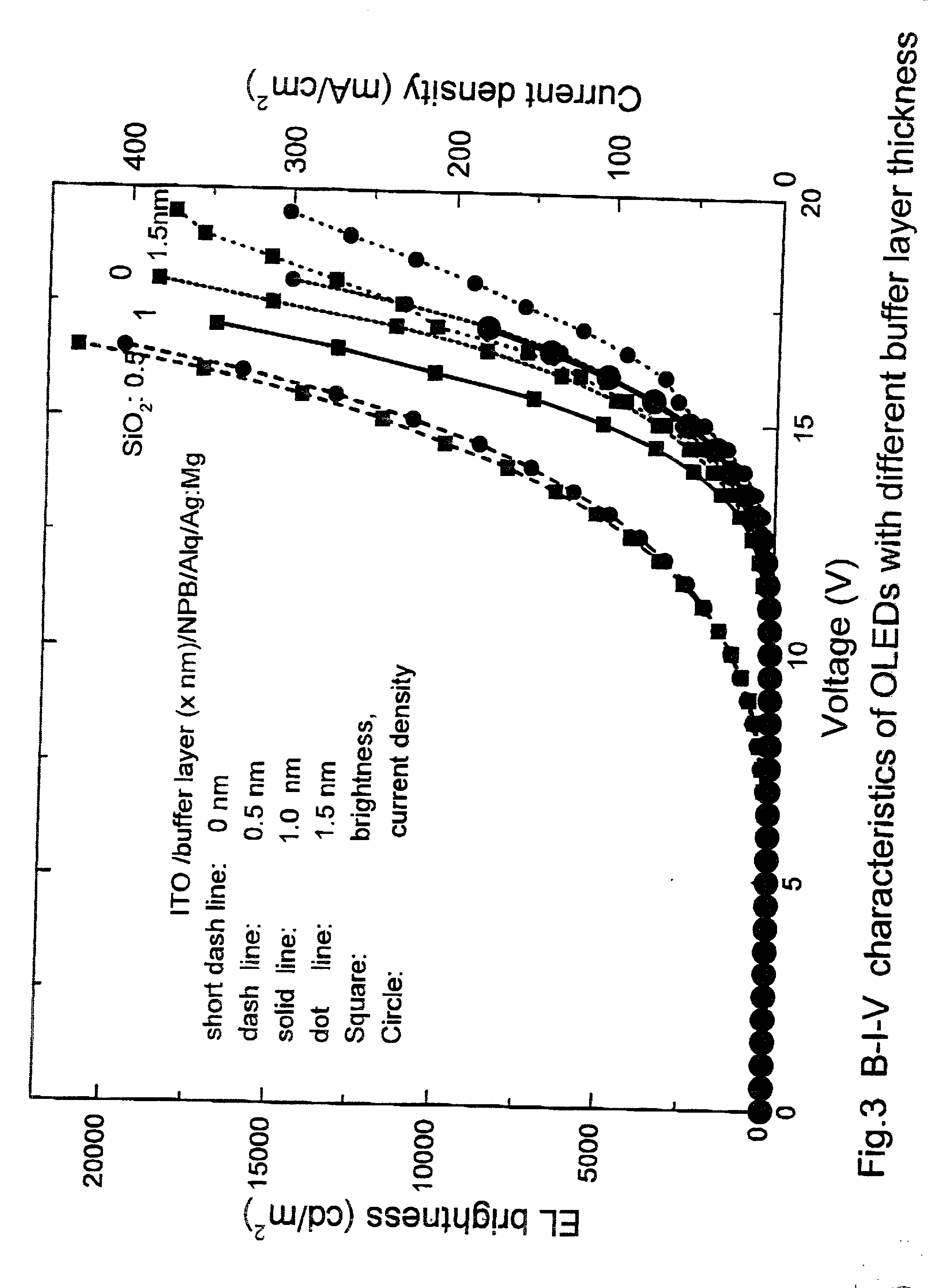
[0033] Brightness-Current-Voltage (B-I-V) Characteristics

[0034] The OELDs were fabricated according to the procedure of Example 1. FIG. 3 shows the B-I-V curves of four devices with different thicknesses of buffer layer (SiO.sub.2)


PUM


Abstract

An organic electroluminescent device (OELD) with improved luminescent efficiency has been fabricated upon inclusion of an inorganic buffer layer in the hole injecting or electron injecting regions. The structure of the device can be as follows (from bottom to top): ITO\buffer layer\NPB\Alq\Mg:Ag. In comparison with devices without the buffer layer, the present OELD may be more efficient in a proper bias condition.

Description

[0001] The present invention pertains to organic thin-film electroluminescent devices and a method of manufacture of such devices.BACKGROUND TO THE INVENTION[0002] Fabrication of organic electroluminescent devices (OELDs) can be traced back to 1960's. Representatives of early OELDs are Gurnee et al U.S. Pat. No. 3,172,862, issued Mar. 9, 1965; Gurnee U.S. Pat. No. 3,173,050, issued Mar. 9, 1965; and Dresner U.S. Pat. No. 3,710,167, issued Jan. 9, 1973. These devices comprised a single organic emitting layer having thicknesses above 1 mm and two electrodes (cathode and anode). Alkali metals were used as the cathode materials as they had the lowest work function values.[0003] Tang et al U.S. Pat. No. 4,356,429 disclosed an OELD with two organic layers, in which the organic luminescent medium consisted of two extremely thin layers separating the anode and the cathode. These comprised one layer injecting and transporting holes and the other layer injecting and transporting electrons and...

Claims


Application Information

Patent Timeline
IPC IPC(8): H01L51/50H01L51/52
CPCH01L51/5088H01L51/5092Y10S428/917H10K50/17H10K50/171
Inventor LEE, SHUIT-TONGDENG, ZHEN-BOGAMBLING, WILLIAM ALEXANDER
Owner CITYU RES
Why Eureka
Try Eureka