Method for forming porous film, insulating film for semiconductor element, and method for forming such insulating film

a technology of insulating film and semiconductor element, which is applied in the direction of vacuum evaporation coating, coating, sputtering coating, etc., can solve the problems of signal delay, failure to reach the relative dielectric constant of 1.5 required by the 0.07 .mu.m design rule of the next generation, and the inability to form a stable porous film

Inactive Publication Date: 2002-03-14
KOMATSU LTD
View PDF0 Cites 15 Cited by
  • Summary
  • Abstract
  • Description
  • Claims
  • Application Information

AI Technical Summary

Problems solved by technology

In the operation of such LSI, a problem is associated with a signal delay proportional to a product of wiring resistance (resistance component) and capacitance between wirings (capacitance components).
However, though the above-described openly disclosed conventional method makes it possible to form a porous film (interlayer insulating film) with a relative dielectric constant of 2.0, it fails to reach a level of relative dielectric constant of 1.5 required by the 0.07 .mu.m design rule of the next generation.
One more problem is that the precursor solution itself undergoes chemical changes and degrades with time, making it impossible to form a stable porous film.
Furthermo

Method used


Image

  • Method for forming porous film, insulating film for semiconductor element, and method for forming such insulating film
  • Method for forming porous film, insulating film for semiconductor element, and method for forming such insulating film
  • Method for forming porous film, insulating film for semiconductor element, and method for forming such insulating film

Examples


Embodiment Construction

[0088] The preferred embodiment of the present invention will be described below with reference to the drawings attached.

[0089] First, a method for forming a porous film will be described.

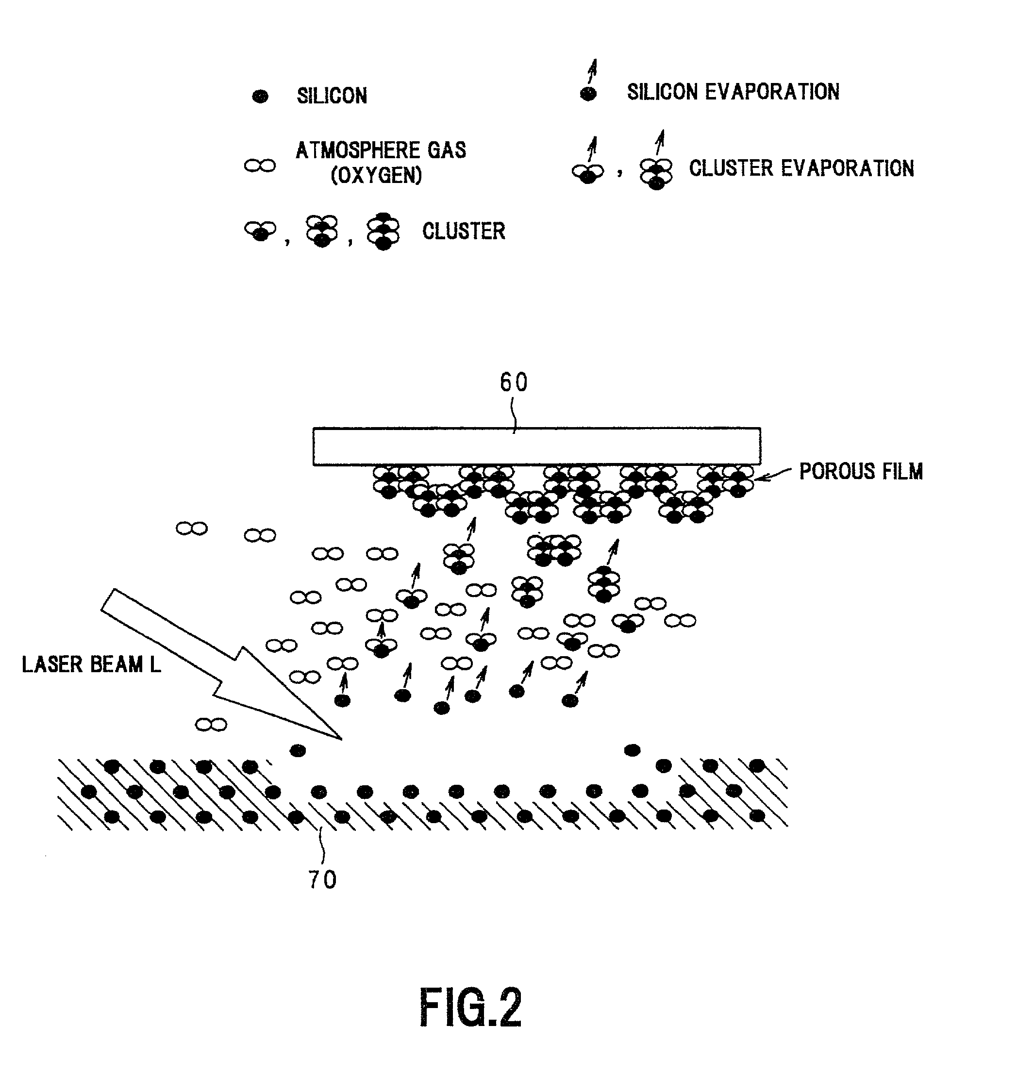
[0090] In the present embodiment, a porous film composed of Si and oxygen and containing pores is formed on a substrate by a laser ablation method using silicon (referred to as Si hereinbelow) in a gas (atmosphere) containing oxygen.

[0091] In accordance with the laser ablation process, a thin film is formed by irradiating a target with a laser (laser beam), thereby heating the surface of the irradiated portion of the target to a high temperature and melting it, causing evaporation of this surface, and inducing the formation of clusters, thereby causing clusters to adhere to the substrate surface.

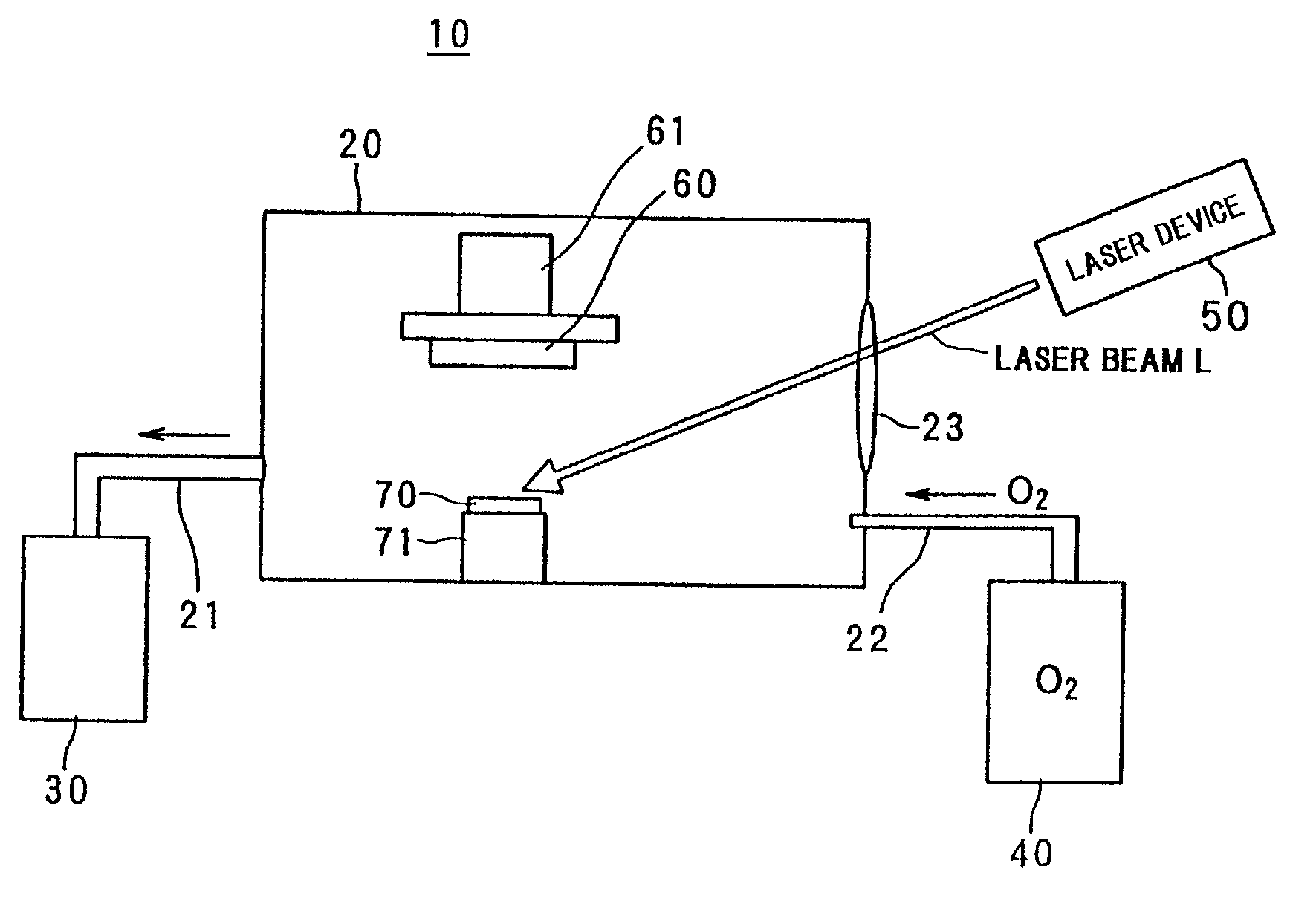
[0092] FIG. 1 is a structural view of an apparatus 10 for implementing the method for forming a porous insulating film in accordance with the present invention.

[0093] As shown in FIG. 1, apparatus 10 is gen...


PUM

PropertyMeasurementUnit
Pressureaaaaaaaaaa
Thicknessaaaaaaaaaa
Pressureaaaaaaaaaa

Abstract

When laser ablation is implemented with respect to a target comprising silicon in an atmosphere containing oxygen, Si constituting the target is ejected from the laser irradiated portion thereof. The ejected Si collides with oxygen, which is the atmosphere gas, and reacts therewith in a gas phase forming clusters composed of SiO2 or SiOx, or silicon (Si) and oxygen, and containing pores with a size of several nanometers. The clusters adhere to the substrate, thereby forming a porous film composed of Si and oxygen and containing pores on the substrate. Furthermore, an insulating film for a semiconductor element is formed to have a multilayer structure in which an aggregate is deposited on the substrate and then a dense film is formed. When the insulating film is formed, the aggregate is produced by implementing laser ablation under a pressure of 1 Kpa, for example. Then, a pressure transition from this 1 KPa to 10 Pa, for example, is caused and a dense film is formed by implementing laser ablation under this pressure of this 10 Pa by adjusting a parameter (for example, laser energy density) other than pressure. The thickness of each layer in the multilayer structure composed of the aggregate and dense film and the thickness ratio of the layers is adjusted by adjusting the number of times the target is irradiated with the laser beam.

Description

[0001] 1. Field of the Invention[0002] The present invention relates to a method for forming a porous film serving as an interlayer insulating film of semiconductors, and also to an insulating film for a semiconductor element having a low relative dielectric constant, and to a method for forming such insulating film.[0003] 2. Description of the Related Art[0004] Conventional semiconductor memory devices, e.g., LSI have been designed and implemented, for example, according to a 0.13 .mu.m or 0.15 .mu.m design rule.[0005] In the operation of such LSI, a problem is associated with a signal delay proportional to a product of wiring resistance (resistance component) and capacitance between wirings (capacitance components). For this reason, it is necessary to decrease the time constant .tau..varies.(C.multidot.R)(C=electrostatic capacitance, R=resistance value) defined by wirings.[0006] For example, as for wiring resistance, the transition from AlCu wiring to Cu wiring resulted in a decre...

Claims


Application Information

Patent Timeline
IPC IPC(8): C23C14/00C23C14/10C23C14/28C23C14/54H01L21/316
CPCC23C14/0021C23C14/10C23C14/28C23C14/54H01L21/02164H01L21/022H01L21/02203H01L21/02269H01L21/31695
Inventor NIRE, TAKASHIMATSUNO, AKIRAKAGAWA, KAZUHIROMUKOUJIMA, MIKA
Owner KOMATSU LTD
Why Eureka
Try Eureka