Support carrier for temporarily attaching integrated circuit chips to a chip carrier and method

a technology of integrated circuit chips and support carriers, which is applied in the field of integrated circuit chip testing, can solve the problems of complex integration circuits, time-consuming and hot process steps, and the need for complex testing means, and achieve the effect of easy movement and easy attachment and detachment of integrated circuit chips

Inactive Publication Date: 2002-04-18
IBM CORP
View PDF0 Cites 10 Cited by
  • Summary
  • Abstract
  • Description
  • Claims
  • Application Information

AI Technical Summary

Benefits of technology

0015] It is another object of the present invention to provide a device for temporarily attaching an integrated circuit chip to a chip carrier for subsequent electrically testing the chip without the need of an additional soldering step.
0016] It is still another object of the present invention to provide such a device that can be easily moved to a test system for further testing.
0017] Furthermore, it is an object of the present invention to provide a method for temporarily attaching an integrated circuit chip to a chip carrier for subsequent electrical testing of the integrated circuit chip that allows easy attaching and detaching of the integrated circuit chip, independent of chip size or type as long as the C4 ball pattern of different chip sizes or types fit to the pad area of the TCA.

Problems solved by technology

As integrated circuits (ICs) have become more complicated, means for testing IC chips have similarly become more complicated and more expensive.
These chips often have several hundred connector pins or even more which challenge the tester to provide complete and secure electrical contact with each pin, in a non-destructive way.
The problem with a TCA is the need for a complex, time consuming and hot process step (soldering) to get the chip mechanically as well as electrically fixed to the TCA and to get it sheared off the TCA after testing has been finished.
Another problem is that in case the chip has to be removed from the final product, e.g., a Multi Chip Module (MCM) to diagnose for failure symptoms, the chip has once more to be attached / soldered to the TCA.
This additional hot process step sometimes results in a NDF (No Defect Found) situation because of unpredictable, self healing effects on the chip under investigation because of the additional hot solder process step.
The devices and methods described in the state of the art as presented heretofore have the disadvantages that they either need additional soldering steps to get the chip electrically and mechanically connected to the test sockets, or they show a complicated design and the chip cannot be removed easily.
Another disadvantage resides in the fact that they do not provide a reliable and easy method of adjusting the chip to the TCA or the chip carrier.

Method used


Image

  • Support carrier for temporarily attaching integrated circuit chips to a chip carrier and method
  • Support carrier for temporarily attaching integrated circuit chips to a chip carrier and method
  • Support carrier for temporarily attaching integrated circuit chips to a chip carrier and method

Examples


Embodiment Construction

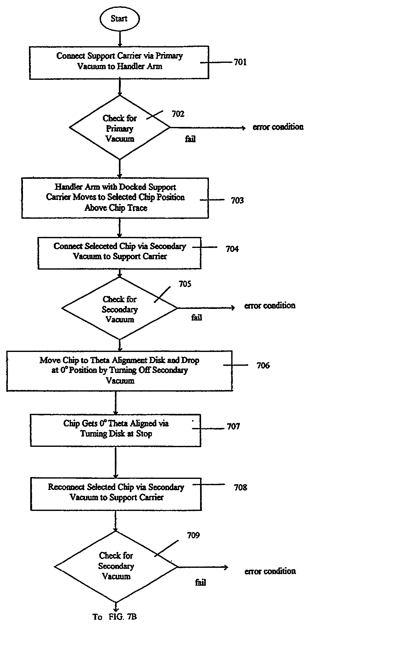
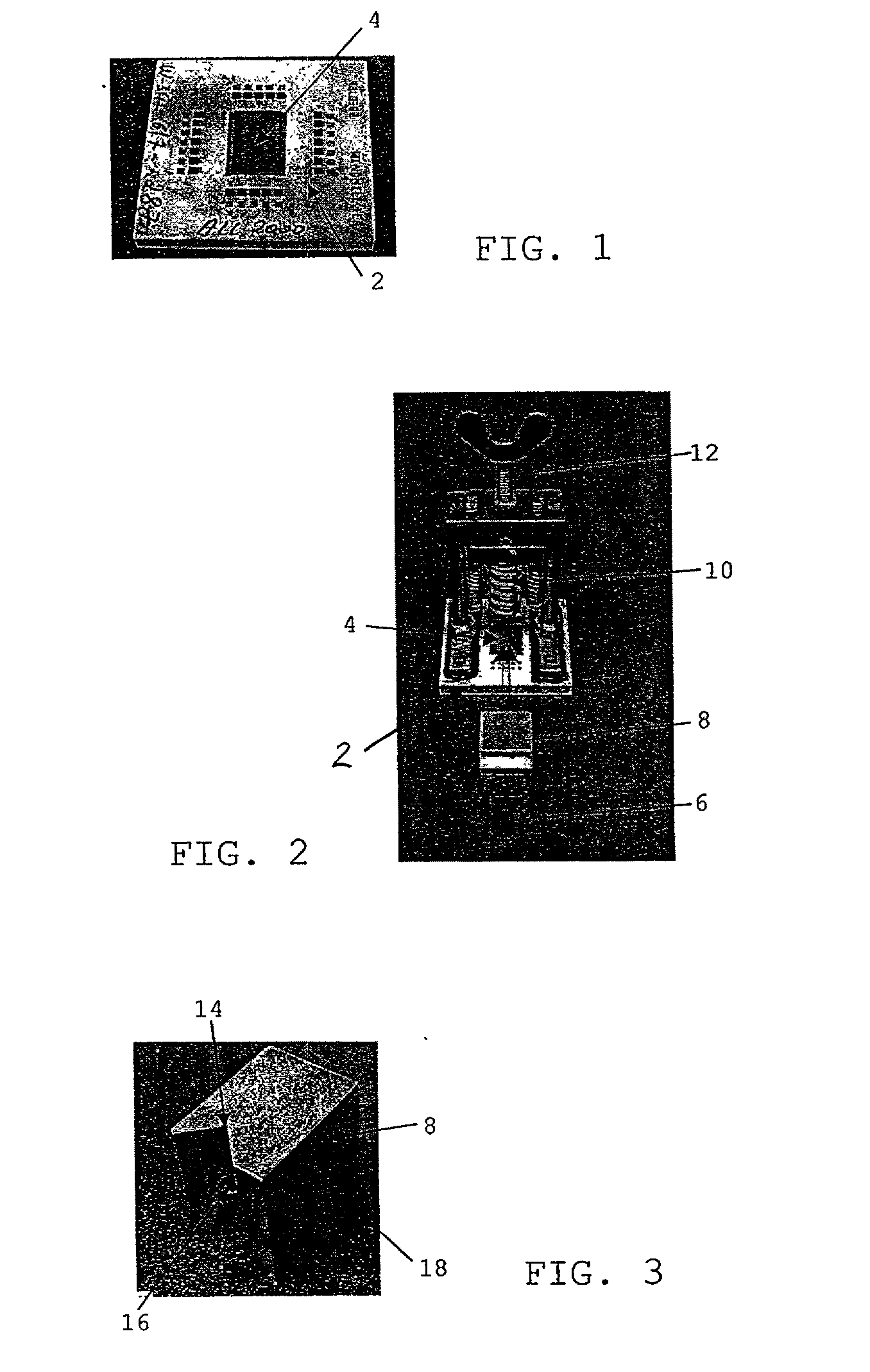
[0027] FIG. 1 shows single chip carrier 2 having pad area 4 used to receive a single chip (not shown) in order to subsequently perform full pin count testing on a test system. The chip to be tested is temporarily attached to the carrier's chip area, usually by a hot process step (soldering step) to get the chip mechanically as well as electrically attached. This soldering step is a complex, time-consuming process and, in addition, the tested chip has to be sheared off the carrier again after testing has been finished. Furthermore, in case of a need to retest the chip these additional process steps will have to be performed several times.

[0028] Another problem arises in case a chip has been removed from the final product, e.g., a Multi Chip Module (MCM), to diagnose the chip for fail symptoms. Then, the chip has to be once again attached / soldered to the single chip carrier. This additional hot process sometimes results in a NDF (No Defect Found) situation because of unpredictable, se...


PUM


Abstract

An apparatus for temporarily attaching an integrated circuit chip to a chip carrier for subsequent electrical testing of the integrated circuit chip is provided consisting of a support carrier and a compression adjusting device to apply a compressive force via the support carrier to the integrated circuit chip to be tested, whereby the support carrier is arranged between the compression adjusting device and the integrated circuit chip to be tested, as well as a method for temporarily attaching an integrated circuit chip to a chip carrier. Furthermore, the support carrier is adapted to function as a transport vehicle for the integrated circuit chip.

Description

[0001] 1. Field of the Invention[0002] The present invention relates to integrated circuit chip testing. More specifically, the invention relates to a temporary connection of the integrated circuit chip to be tested to a chip carrier.[0003] 2. Background of the Invention[0004] As integrated circuits (ICs) have become more complicated, means for testing IC chips have similarly become more complicated and more expensive. These chips often have several hundred connector pins or even more which challenge the tester to provide complete and secure electrical contact with each pin, in a non-destructive way. Accordingly, cost effective chip development requires chip test fixtures that provide for non-destructive, easy installation and removal of the chip from the test device.[0005] Today's state of the art principle to test high pin count chips with area footprint and C4 (flip chip) technology, after low pin count wafer test has been executed and the chip has been diced for further full pin...

Claims


Application Information

Patent Timeline
Patent Type & Authority Applications(United States)
IPC IPC(8): G01R1/04
CPCG01R1/0433
Inventor TORREITER, OTTO ANDREAS
Owner IBM CORP
Why Eureka
Try Eureka