Organic luminescence display device and process for production thereof

a luminescence display and organ technology, applied in the direction of identification means, instruments, adhesive processes with surface pretreatment, etc., can solve the problems of poor durability of film laminate structure, difficult to produce high-definition full-color display panels, and subjected sealing

Inactive Publication Date: 2002-05-09
CANON KK
View PDF15 Cites 70 Cited by
  • Summary
  • Abstract
  • Description
  • Claims
  • Application Information

AI Technical Summary

Problems solved by technology

Such a film laminate structure is generally poor in durability against moisture and heat and is therefore subjected to sealing as by covering entirely with a photocurable resin and applying a glass sheet thereto (JP-A 6-338392), by placing the structure within a vessel of glass, etc., having an injection port and injecting a liquid sealant through the injection port for sealing (JP-A 7-11247), or by covering with a laminate film which has been used as a means for sealing an inorganic EL device (JP-A 60-14798).
According to these processes, however, it has been difficult to produce a high-definition full-color display panel because of the restriction by positional accuracy and aperture size of the shadow mask.
For alleviating the difficulty, JP-A 9-167684 has proposed a process including a patterning method using a donor sheet but the process becomes complicated as a whole since it requires vacuum deposition for formation of luminescence layers.
However, it is generally difficult to uniformly form organic film layers, and the surface planarity of the resultant film layers changes with time and temperature, so that it becomes furthermore difficult to form a metal layer on the organic film layers.
Further, even if the organic film layers are successfully uniformly formed, the subsequent metal layer formation thereon is liable to damage the organic film layers because of a high energy of the metal layer formation.
These difficulties are led to fluctuation of laminate film layer thickness and occurrence of pinholes, resulting in a remarkable lowering in luminescence performances.
However, the dispersion of an organic EL material in a binder resin is liable to remarkably lower then luminescence efficiency and the efficiency of injection or transportation of electrons or holes, thus increasing the amount of electricity for the operation.
Further, the application of different layers is liable to result in a peeling at the application boundary.

Method used


Image

  • Organic luminescence display device and process for production thereof
  • Organic luminescence display device and process for production thereof
  • Organic luminescence display device and process for production thereof

Examples


example 2

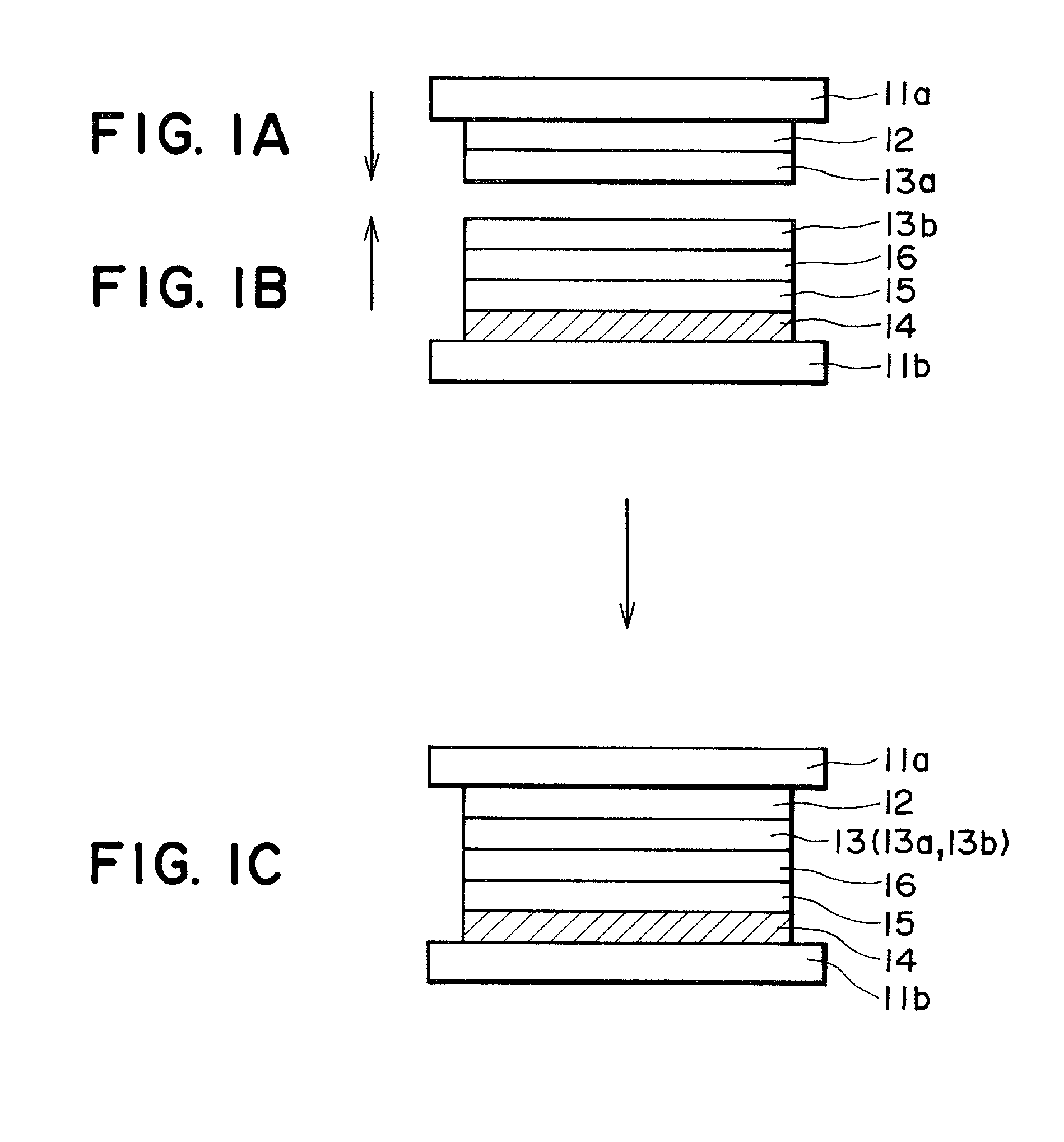
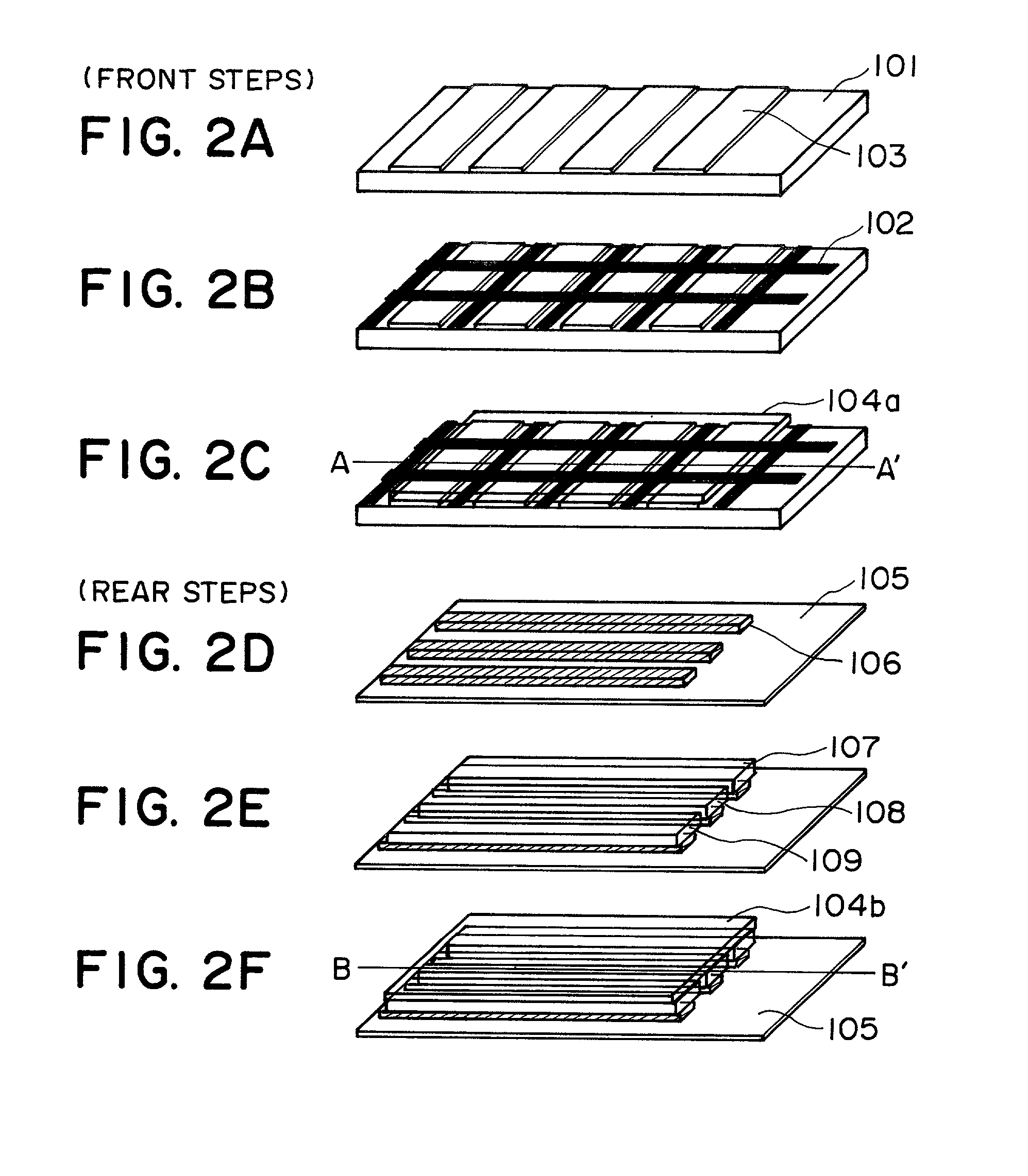
[0064] A direct viewing-type passive full-color organic luminescence display device was prepared through steps as shown in FIGS. 2A through 2J, similarly as in Example 1, except that a pre-baking step was inserted before the application of the two substrates.

[0065] Thus, referring to FIGS. 2A-2J, a glass substrate 101 (as a front substrate) was first provided with ITO transparent electrodes 103 by vacuum deposition (FIG. 2A) and then provided with a resinous black matrix 102 of a high-resistivity black resist (made by Fuji Film Olin K.K.) through a lithographic process (FIG. 2B). Separately, a 0.5 wt. % in toluene of TPA-6 was applied by extrusion coating. The thus-treated front substrate 101 was prebaked at 40.degree. C. to form a 0.05 .mu.m-thick first hole-injection layer 104a (FIG. 2C) and stored in a dry nitrogen gas atmosphere.

[0066] Separately, a rear glass substrate 105 was provided with Al metal electrodes 106 (FIG. 2D), and then provided with 0.05 .mu.m-thick luminescence ...

example 3

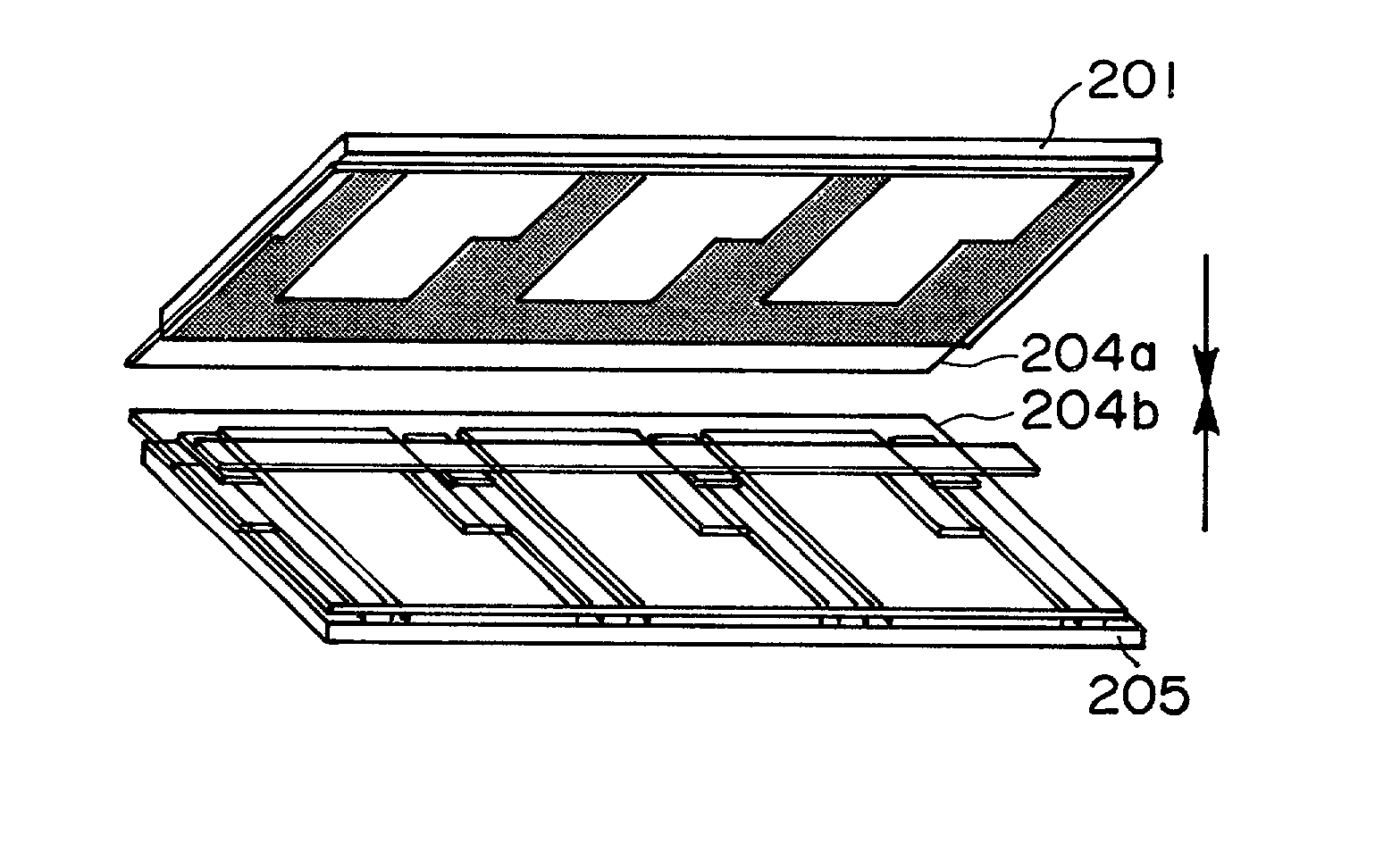
[0069] A direct viewing-type passive full-color organic luminescence display device was prepared through steps as shown in FIGS. 3A through 3H.

[0070] Referring to these figures, a glass substrate 201 (as a front substrate) was first provided with a resinous black matrix 202 of a high-resistivitity black resist (made of Fuji Film Olin K.K.) (FIG. 3A) and then with ITO transparent electrodes 203 by vacuum deposition (FIG. 3B), which was then coated by extrusion coating with a 0.5 wt. %-solution in toluene of TPA-6, followed by pre-baking at 40.degree. C., to form a 0.05 .mu.m-thick first hole-injection layer 204a (FIG. 4C). The front substrate 201 thus-treated was then stored in a dry nitrogen atmosphere.

[0071] Separately, a rear glass substrate 205 was first provided with metal electrodes 205 each having a laminate structure of an Al--Li alloy layer on an Al layer (FIG. 3D), and then successively provided with thin film transistors 210, data electrodes 211, an insulating layer 213 an...


PUM

PropertyMeasurementUnit
luminanceaaaaaaaaaa
temperatureaaaaaaaaaa

Abstract

An organic luminescence device including organic layers disposed between an anode and a cathode is produced through a process including: a step of forming a first organic layer over an anode already formed on a first substrate; a step of forming a second organic layer comprising an identical material forming the first organic layer over a cathode already formed on a second substrate; and a combining step of disposing the first and second organic layers opposite to each other and applying the first and second organic layer to each other under pressure, followed by baking, to form a laminate organic luminescence device. A step of pre-baking at least one of the first and second organic layers is preferably included prior to the combining step. As a result, the organic layers in the luminescence device can be formed free from binders and yet in a good adhesion therebetween.

Description

FIELD OF THE INVENTION AND RELATED ART[0001] The present invention relates to an organic luminescence (display) device formed by application of separately prepared two substrates and a process for production thereof.[0002] An organic luminescence device (hereinafter sometimes also called an "organic EL device") has a structure including a cathode, an anode, and a film comprising a fluorescent organic compound sandwiched between the cathode and the anode. In the organic luminescence device, electron and holes are injected into the film and re-combined therein to form excitons, which are then caused to emit light (fluorescence or / and phosphorescence) at the time of deactivation thereof thus causing luminescence.[0003] Such an organic EL device is characterized by a capability of luminescence at a high luminance on the order of 10.sup.2-10.sup.5 cd / m.sup.2 at a low voltage of 10 vols or lower and also by a capability of blue to red luminescence by selection of fluorescent materials.[00...

Claims


Application Information

Patent Timeline
Patent Type & Authority Applications(United States)
IPC IPC(8): G09F9/00G09F9/30H05B33/10H01L27/32H01L51/50H05B33/04H05B33/12
CPCH01L27/3244H01L27/3281H01L51/56H01L51/5284H01L51/0024H10K59/17H10K71/50H10K59/12H10K50/865H10K71/00
Inventor ISHIKAWA, NOBUYUKIYONEMOTO, ISSEIMIDORIKAWA, SATOKOSAITO, YASUYUKI
Owner CANON KK
Why Eureka
Try Eureka