Method of forming insulating film and process for producing semiconductor device

a technology of insulating film and semiconductor, which is applied in the direction of transportation and packaging, coating, layered products, etc., can solve the problems of poor cracking resistance, affecting device operation frequency and power consumption, and difficult to use this film as a single-layer interlayer dielectric in lsi

Inactive Publication Date: 2002-07-04
KK TOSHIBA +1
View PDF0 Cites 18 Cited by
  • Summary
  • Abstract
  • Description
  • Claims
  • Application Information

AI Technical Summary

Problems solved by technology

In semiconductor devices, wiring resistance and wiring capacitance are increasing steadily with the trend toward wiring size reduction, and this is coming to considerably influence the operating frequency and power consumption of devices.
The film thus obtained has poor cracking resistance and, hence, it has been difficult to use this film as a single-layer interlayer dielectric in LSI's.
Because of this, it has been exceedingly difficult to use organosilicon oxide films in a wide range of applications as an interlayer dielectric for multilayered wiring structures comprising five or more layers for use in high-performance semiconductor devices.
However, in case where the first polymer has t

Method used


Image

  • Method of forming insulating film and process for producing semiconductor device
  • Method of forming insulating film and process for producing semiconductor device
  • Method of forming insulating film and process for producing semiconductor device

Examples


example 2

[0143] In this Example, interlayer dielectrics each consisting of an organosilicon oxide film were formed from a mixture of a first polymer and a second polymer in various proportions (by weight). A copper damassin wiring was further formed thereon to produce semiconductor devices. The organosilicon oxide films were examined for a change in dielectric constant caused by an O.sub.2 plasma.

[0144] FIG. 7 shows sectional views illustrating steps of the semiconductor device production process used in this Example.

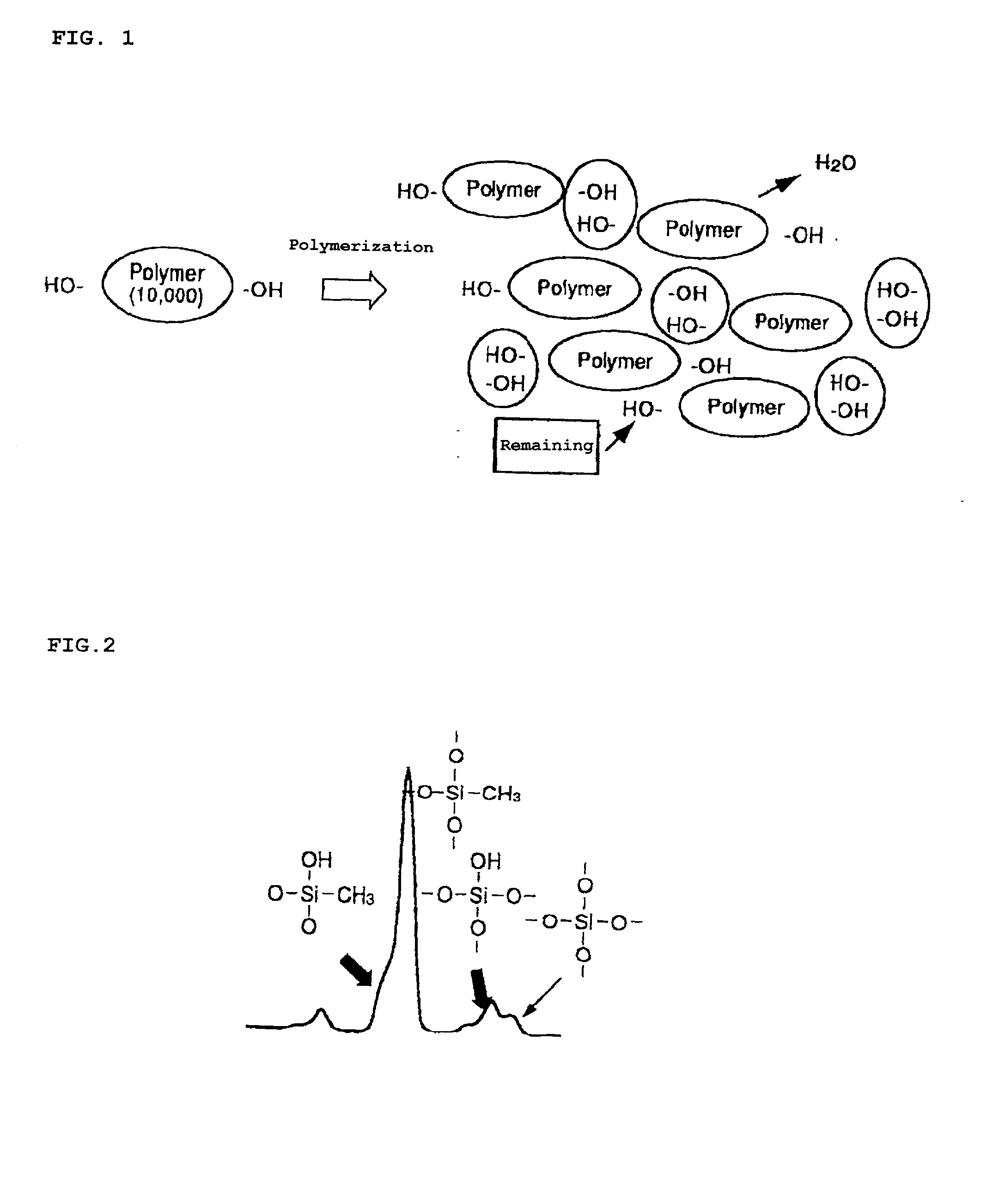
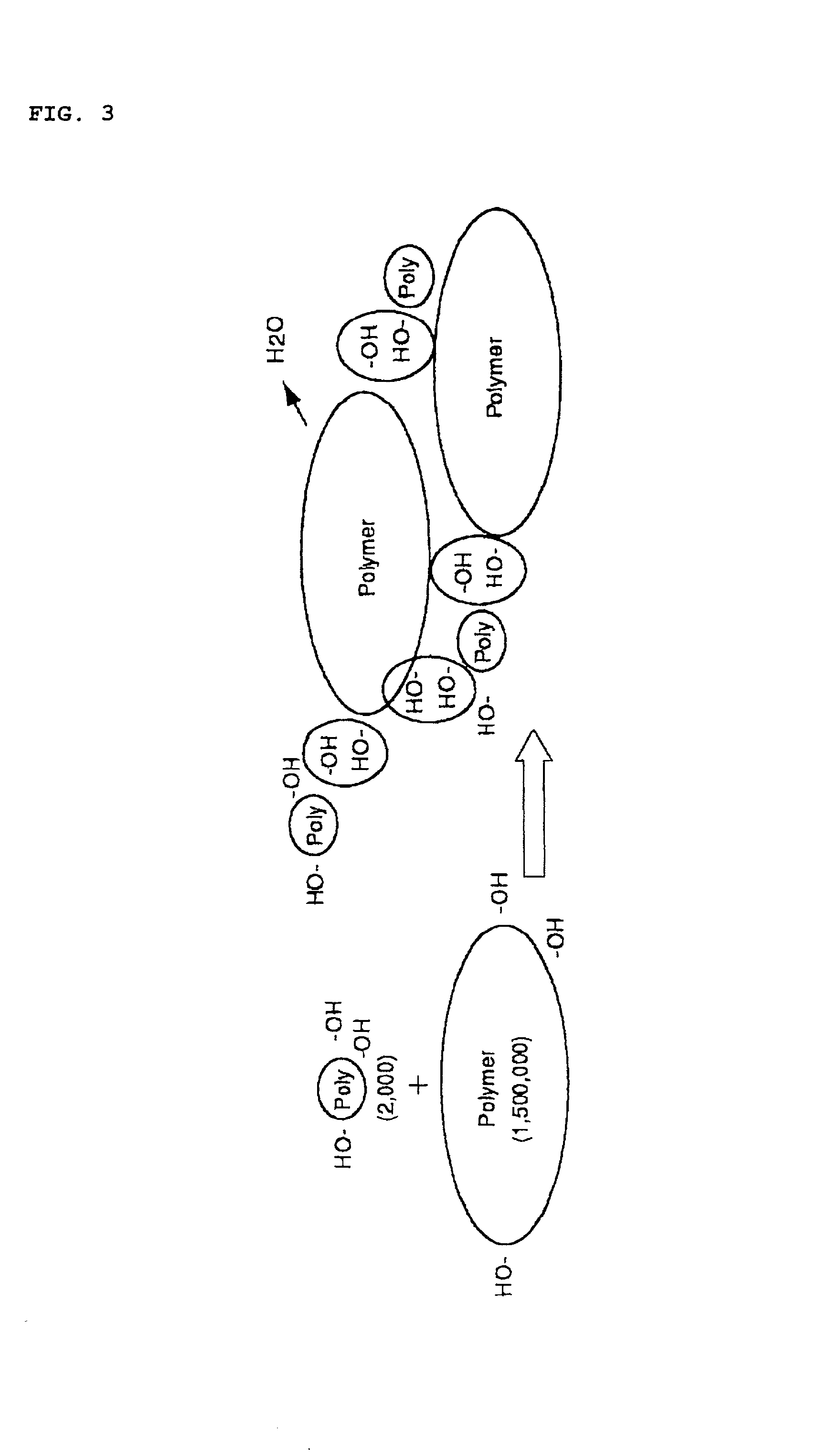
[0145] First, an interlayer dielectric 22 comprising an organosilicon oxide film was formed on a silicon substrate 21 having elements (not shown) formed thereon, as shown in FIG. 7A. The organosilicon oxide film was formed in the following manner. First, methylpolysiloxane having a weight average molecular weight of 1,000,000 as a first polymer having a high molecular weight and methylpolysiloxane having a weight average molecular weight of 10,000 as a second polymer having a lo...

example 3

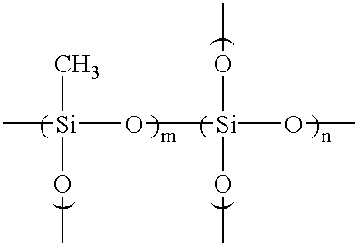
[0157] A chemical solution was prepared by dissolving methylpolysiloxane having a weight average molecular weight of 2,000,000 as a first polymer, methylpolysiloxane having a weight average molecular weight of 2,000 as a second polymer, and methylpolysiloxane having a weight average molecular weight of 20,000 as a third polymer in cyclohexanone as a solvent. The first, second and third polymers were used in a proportion of 30 / 20 / 50 by weight. The polymers used here each were a compound represented by general formula (1) wherein CH.sub.3 / Si was 0.72.

[0158] An interlayer dielectric comprising an organosilicon oxide film was formed on a silicon substrate having a buried copper wiring in the same manner as in Example 2, except that the chemical solution obtained above was used.

[0159] In the interlayer dielectric thus formed, no unevenness in film quality was observed. This interlayer dielectric was a homogeneous film. It is thought that due to the use of the three polymers differing in ...


PUM

PropertyMeasurementUnit
Angleaaaaaaaaaa
Percent by massaaaaaaaaaa
Temperatureaaaaaaaaaa

Abstract

A method of forming an insulating film which includes the steps of: dissolving in a solvent a first and second polymer which each comprise methylpolysiloxane as the main component and one of which has a weight average molecular weight at least 10 times that of the other to thereby prepare a chemical solution; applying the chemical solution to a semiconductor substrate to form a coating film; and heat-treating the coating film to thereby form an organosilicon oxide film. The weight-average molecular weight of the first polymer is preferably at least 100 times that of the second polymer. Thus, an insulating organosilicon oxide film having a low dielectric constant and high cracking resistance is formed from a coating fluid.

Description

CROSS-REFERENCE TO THE RELATED APPLICATION[0001] This application is a continuation-in-part application of Application No. 09 / 670,547, filed Sep. 27, 2000, entitled "COMPOSITION FOR FILM FORMATION, METHOD OF FILM FORMATION, AND INSULATING FILM", now pending.[0002] The present invention relates to a method of forming an insulating film, more particularly, a method of forming a low dielectric constant insulating film by a coating method. The invention further relates to a process for producing a semiconductor device using the insulating film as an interlayer dielectric.DESCRIPTION OF THE RELATED ART[0003] In semiconductor devices, wiring resistance and wiring capacitance are increasing steadily with the trend toward wiring size reduction, and this is coming to considerably influence the operating frequency and power consumption of devices. Investigations are hence being made enthusiastically on the use of organosilicon oxide films or organic films formed from a coating fluid as interl...

Claims


Application Information

Patent Timeline
IPC IPC(8): H01L21/312
CPCC08G77/16C09D183/06H01L21/02126H01L21/02216H01L21/02282H01L21/3122Y10T428/31663
Inventor NAKATA, REMPEIYAMADA, NOBUHIDEMIYAJIMA, HIDESHIKOJIMA, AKIHIROKUROSAWA, TAKAHIKOHAYASHI, EIJISEO, YOUNGSOONSHIOTA, ATSUSHIYAMADA, KINJI
Owner KK TOSHIBA
Why Eureka
Try Eureka