

Semiconductor device and liquid crystal module using the same
a technology of liquid crystal module and semiconductor device, which is applied in the direction of identification means, instruments, optics, etc., can solve the problems of fine process unsuitable for manufacturing the driver part, arrangement cannot meet the requirement to produce finer liquid crystal panel, etc., and achieve the effect of reducing the pitch of the terminal
- Summary
- Abstract
- Description
- Claims
- Application Information
AI Technical Summary
Benefits of technology
Problems solved by technology
Method used
Image

Examples
first embodiment
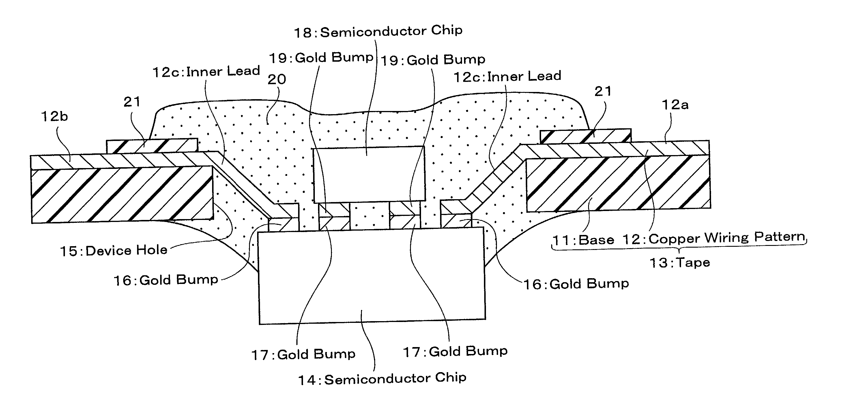
[0034] The following description will discuss a first embodiment in accordance with the present invention in reference to FIGS. 1 to 7.
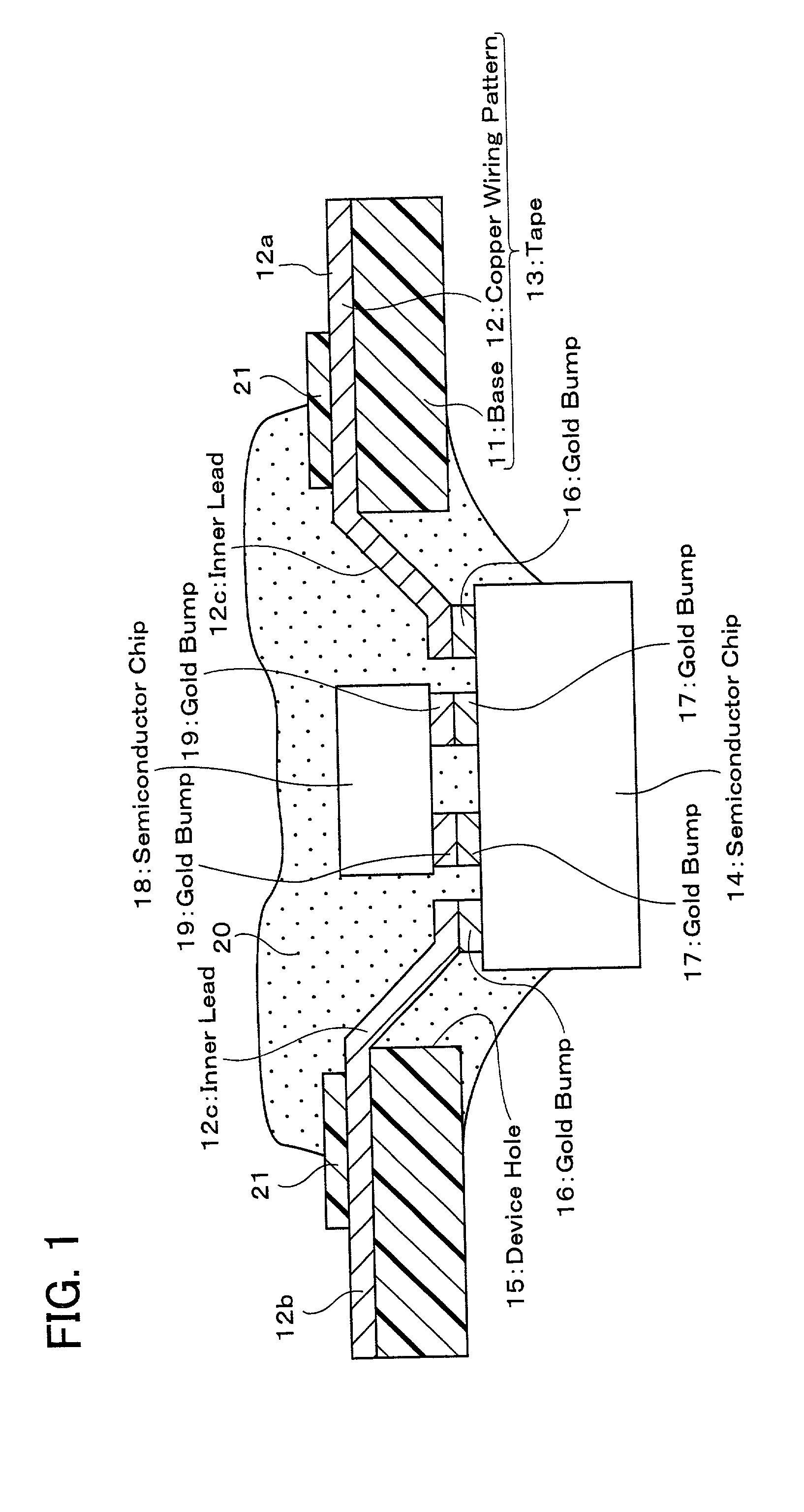
[0035] FIG. 1 is a cross-sectional view of a semiconductor device in accordance with a first embodiment of the present invention. FIGS. 2 to 4 are plan views of FIG. 1, and FIG. 4 indicates a cutting plane of FIG. 1 with referential signs A-A.
[0036] A tape (tape carrier) 13 is arranged by providing a copper wiring pattern 12 on a base 11 made of organic materials such as polyimide. Extending parts 12a and 12b of the copper wiring pattern 12 extend from the periphery of the base 11 to be in parallel with each other. The extending part 12a is connected to, for instance, a pad of a liquid crystal panel via an anisotropic conductive film etc., whereas the extending part 12b is connected to, for instance, a power source and a pad of a printed board to which an image data signal is transmitted. The parts are electrically and mechanically connected. A liqui...
second embodiment
[0051] The following description will discuss a second embodiment in accordance with the present invention in reference to FIGS. 8 and 9.
[0052] FIGS. 8 and 9 are cross-sectional view showing semiconductor devices of the second embodiment of the present invention. These semiconductor devices are similar to the aforementioned device so that members equivalent to the aforementioned ones have the same signs and the definitions are omitted.
[0053] It is noted that in the semiconductor device shown in FIGS. 8 and 9, a semiconductor chip 31 mounted on a tape 13 by ILB is a liquid crystal driver IC for driving a segment electrode of a liquid crystal panel, and a semiconductor chip 32, which is a liquid crystal driver IC for driving a common electrode, is bonded on the semiconductor chip 31, and further a semiconductor chip 33, which is an SRAM, is bonded on the semiconductor chip 32.
[0054] On this account, as in the case above, a gold bump 16 of the semiconductor chip 31 is connected to an i...
third embodiment
[0058] The following description will discuss a third embodiment in accordance with the present invention in reference to FIGS. 10 and 11.
[0059] FIGS. 10 and 11 are cross-sectional views showing semiconductor devices of the third embodiment of the present invention. These semiconductor devices are similar to the device shown in FIGS. 8 and 9 so that members equivalent to the aforementioned ones have the same sign and the definitions are omitted.
[0060] It is noted that in the semiconductor device shown in FIGS. 10 and 11, a semiconductor chip 41, which is a controller IC, is further bonded on a semiconductor chip 33.
[0061] Similarly to the semiconductor chip 33, by a dicing sheet 42, the back surface of the semiconductor chip 41 is, as shown in FIG. 10, bonded to an area on the semiconductor chip 33, which is surrounded by aluminum pads 35. The aluminum pad 43 is bonded with an inner lead 12c via a gold wire 44.
[0062] In the arrangement shown in FIG. 11, meanwhile, similarly to the s...
PUM
| Property | Measurement | Unit |
|---|---|---|
| pressure | aaaaa | aaaaa |
| temperature | aaaaa | aaaaa |
| thickness | aaaaa | aaaaa |
Abstract
Description
Claims
Application Information