Method for producing an organic light emitting device (OLED) and structure produced thereby

a light emitting device and organic technology, applied in the direction of organic semiconductor devices, solid-state devices, thermoelectric devices, etc., can solve the problems of low light transmission efficiency,

Inactive Publication Date: 2002-08-29
INNOLUX CORP
View PDF0 Cites 14 Cited by
  • Summary
  • Abstract
  • Description
  • Claims
  • Application Information

AI Technical Summary

Benefits of technology

[0015] It is another object of the present invention to provide a new and improved method for production of an organic light emitting device, array and display based thereon by avoiding the before mentioned disadvantages.
[0016] It is yet another object of the present invention to provide organic light emitting devices having a large light emitting area of uniform brightness, a long service life, and easy and low-cost manufacturing of the same.
[0017] In a first aspect of the present invention, a structure and method is provided for producing an organic light emitting device having a multilayered structure with a substrate providing a first electrode layer, a second electrode layer and at least one layer of light emitting organic material between said first and second electrode layers. The second electrode layer includes at least two separate layers including a layer of a semi-transparent metal electrode (TME) and a layer of transparent lateral conductor (TLC). The layer of a semi-transparent metal electrode is deposited onto the layer of light emitting organic material. At least one light transparent layer being not light emitting (e.g., opaque) is deposited on the semi-transparent metal electrode (TME), to provide protection against the effects of a following deposition of the layer of light transparent conductive material (the transparent lateral conductor (TLC)).
[0018] The protection layer shields the light emitting organic material layer and the semi-transparent metal electrode (TME) from damage caused by the deposition process such as sputtering or evaporation of ITO under oxygen atmosphere.
[0025] With the inventive method, a highly, transparent common top electrode can be deposited without damaging the areas of the active organic layers. The electrical contact from the transparent lateral conductor to the lighting pixel area is made via the space between the pixels where the TLC is in contact with the semi-transparent metal electrode. With this process, large area displays can be fabricated, because the semi-transparent metal electrode is highly transparent and sufficiently thick enough to supply enough current for one pixel. The high current density occurs in the thick transparent lateral conductor which supplies current for the entire display.

Problems solved by technology

However, the deposition of such a transparent lateral conductor (TLC) causes problems, especially for large area organic light emitting displays for the following reasons.
However, this relatively aggressive sputter process damages the underlying organic materials or even shorts to the bottom electrode.
Secondly, commonly-used transparent lateral conductors are metal oxides.
During evaporation of suitable metals under an oxygen-rich atmosphere the organic materials are likely to degrade.
Thirdly, alternative suitable materials for transparent lateral conductors and processes which can be deposited very gently and can exhibit high transmittance and high conductivity are not known so far.
But for large areas, this semi-transparent metal electrode is not conductive enough to supply the high current needed to illuminate all pixels.
However, making the semi-transparent metal electrode thicker would result in unacceptably high absorption of the light and consequently lead to a significantly reduced luminous inefficiency of the device.

Method used


Image

  • Method for producing an organic light emitting device (OLED) and structure produced thereby
  • Method for producing an organic light emitting device (OLED) and structure produced thereby

Examples


Embodiment Construction

[0029] Referring now to the drawings, and more particularly to FIGS. 1-2, there is shown a preferred embodiment of the method and structures according to the present invention.

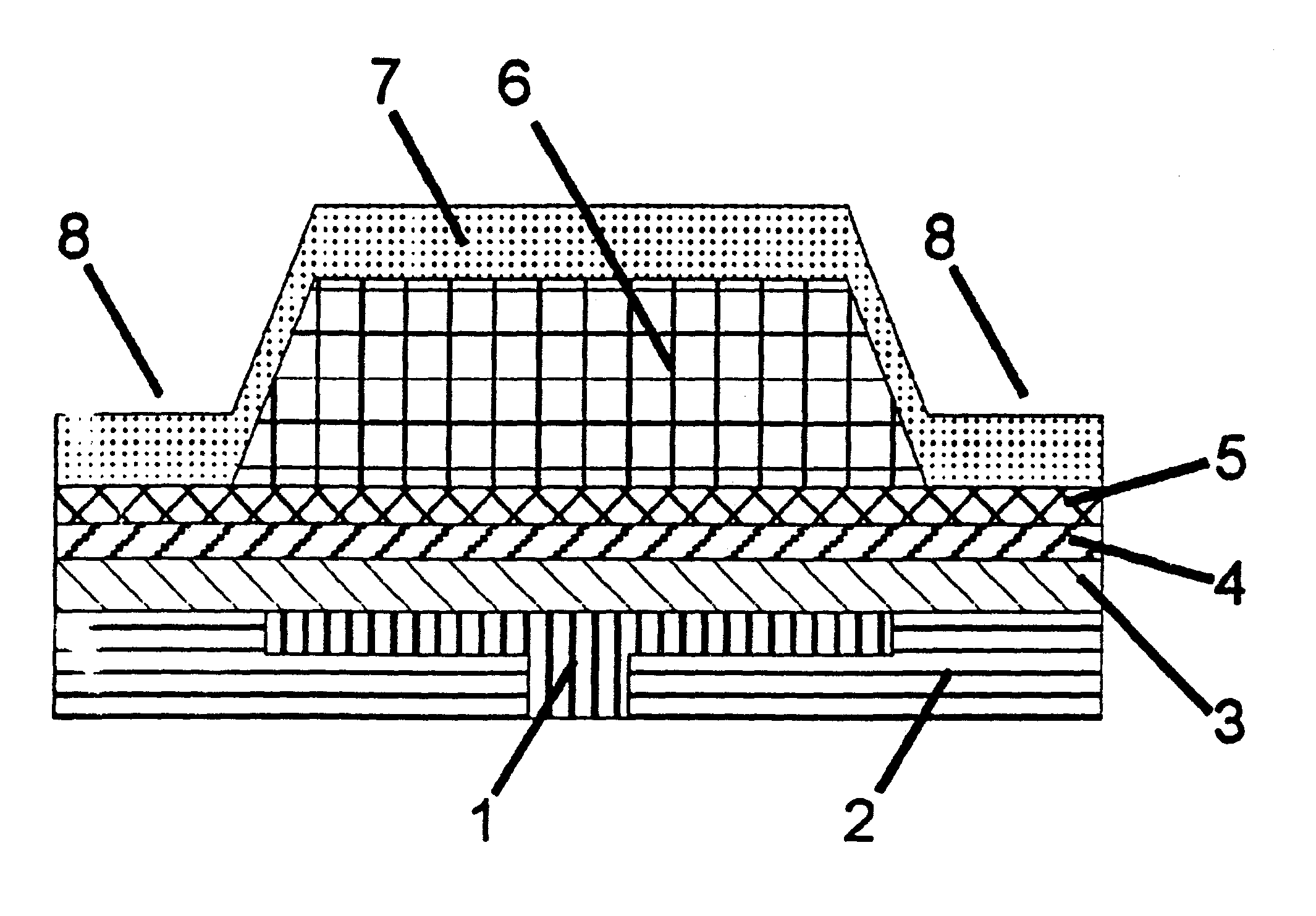
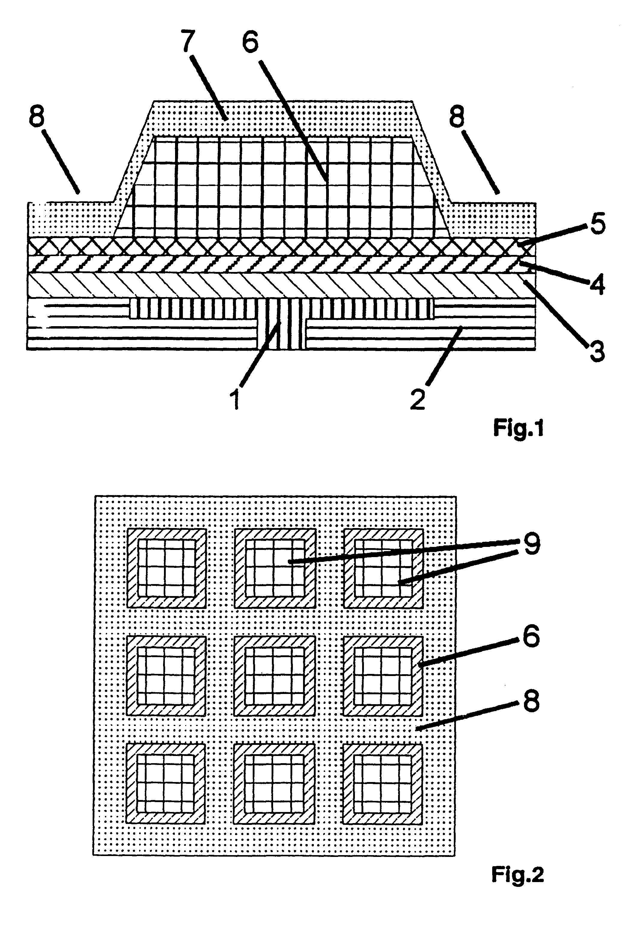
[0030] FIG. 1 shows an exemplary cross-section of a pixel element of an organic display. The pixel of an organic display is defined by an electrode pad 1 made of metal which acts as the anode.

[0031] The electrode pad 1 is integrated into the surface of the substrate 2 and connected to the integrated driving circuit (not shown). A stack of organic layers 3 are successively deposited on top of the substrate 2 covering also the electrode pad 1 and completed with a 5-nm thin layer 4 of Ca being the cathode and representing the layer of conductive material 4 (e.g., also called "the semi-transparent metal electrode (TME)"). A 20-nm GaN film 5 is deposited to protect the Ca layer 4 from oxidation and the subsequent deposition process of the second protection layer.

[0032] A photoresist 6 is formed (e.g., spun) on the ...


PUM


Abstract

An organic light emitting device (and a method for producing the device) includes a multilayered structure with a substrate layer providing a first electrode layer, a second electrode layer and at least one layer of light emitting organic material between the first and second electrode layers. The second electrode layer includes at least two separate layers, a layer of a semi-transparent metal electrode and a layer of light transparent lateral conductor, is deposited onto the layer of light emitting organic material such as depositing the semi-transparent metal electrode layer onto the layer of light emitting organic material, depositing subsequently at least one protection layer thereupon and depositing the light transparent lateral conductor layer onto the protection layer.

Description

[0001] 1. Field of the Invention[0002] The present invention relates to a method for producing an organic light emitting device, such as organic light emitting diodes (OLEDs), a multi-color display and the like, having a multilayered structure with a substrate layer providing a first electrode layer, a second electrode layer, and at least one layer of light emitting organic material between the first and second electrode layers. Further, the invention is directed to a structure of an organic light emitting diode.[0003] 2. Description of the Related Art[0004] Organic light emitting diodes (OLEDs) are an emerging technology with potential applications as discrete light emitting devices, or as the active element of light emitting arrays or displays, such as flat-panel displays. OLEDs are devices in which a stack of organic layers is sandwiched between two electrodes. At least one of the electrodes must be transparent in order for light, which is generated in the active region of the or...

Claims


Application Information

Patent Timeline
Patent Type & Authority Applications(United States)
IPC IPC(8): H01L27/32H01L51/52
CPCH01L27/3281H01L51/5203H01L51/5221H01L51/5262H01L2251/5315H10K59/17H10K50/805H10K50/82H10K50/85H10K2102/3026
Inventor BEIERLEIN, TILMAN A.
Owner INNOLUX CORP
Why Eureka
Try Eureka